
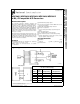
User Manual
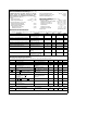

Absolute Maximum Ratings (Notes1&2)
If Military/Aerospace specified devices are required,
please contact the National Semiconductor Sales
Office/Distributors for availability and specifications.
Supply Voltage (V
CC
) (Note 3) 6.5V
Voltage
Logic Control Inputs
b
0.3V to
a
18V
At Other Input and Outputs
b
0.3V to (V
CC
a
0.3V)
Lead Temp. (Soldering, 10 seconds)
Dual-In-Line Package (plastic) 260
§
C
Dual-In-Line Package (ceramic) 300
§
C
Surface Mount Package
Vapor Phase (60 seconds) 215
§
C
Infrared (15 seconds) 220
§
C
Storage Temperature Range
b
65
§
Cto
a
150
§
C
Package Dissipation at T
A
e
25
§
C 875 mW
ESD Susceptibility (Note 10) 800V
Operating Ratings (Notes1&2)
Temperature Range T
MIN
s
T
A
s
T
MAX
ADC0801/02LJ, ADC0802LJ/883
b
55
§
C
s
T
A
s
a
125
§
C
ADC0801/02/03/04LCJ
b
40
§
C
s
T
A
s
a
85
§
C
ADC0801/02/03/05LCN
b
40
§
C
s
T
A
s
a
85
§
C
ADC0804LCN 0
§
C
s
T
A
s
a
70
§
C
ADC0802/03/04LCV 0
§
C
s
T
A
s
a
70
§
C
ADC0802/03/04LCWM 0
§
C
s
T
A
s
a
70
§
C
Range of V
CC
4.5 V
DC
to 6.3 V
DC
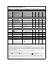
Electrical Characteristics
The following specifications apply for V
CC
e
5V
DC
,T
MIN
s
T
A
s
T
MAX
and f
CLK
e
640 kHz unless otherwise specified.
Parameter Conditions Min Typ Max Units
ADC0801: Total Adjusted Error (Note 8) With Full-Scale Adj.
g
(/4 LSB
(See Section 2.5.2)
ADC0802: Total Unadjusted Error (Note 8) V
REF
/2
e
2.500 V
DC
g
(/2 LSB
ADC0803: Total Adjusted Error (Note 8) With Full-Scale Adj.
g
(/2 LSB
(See Section 2.5.2)
ADC0804: Total Unadjusted Error (Note 8) V
REF
/2
e
2.500 V
DC
g
1 LSB
ADC0805: Total Unadjusted Error (Note 8) V
REF
/2-No Connection
g
1 LSB
V
REF
/2 Input Resistance (Pin 9) ADC0801/02/03/05 2.5 8.0 kX
ADC0804 (Note 9) 0.75 1.1 kX
Analog Input Voltage Range (Note 4) V(
a
)orV(
b
) Gnd– 0.05 V
CC
a
0.05 V
DC
DC Common-Mode Error Over Analog Input Voltage
g
(/16
g
(/8 LSB
Range
Power Supply Sensitivity V
CC
e
5V
DC
g
10% Over
g
(/16
g
(/8 LSB
Allowed V
IN
(
a
) and V
IN
(
b
)
Voltage Range (Note 4)
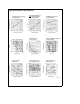
AC Electrical Characteristics
The following specifications apply for V
CC
e
5V
DC
and T
A
e
25
§
C unless otherwise specified.
Symbol Parameter Conditions Min Typ Max Units
T
C
Conversion Time f
CLK
e
640 kHz (Note 6) 103 114 ms
T
C
Conversion Time (Note 5, 6) 66 73 1/f
CLK
f
CLK
Clock Frequency V
CC
e
5V, (Note 5) 100 640 1460 kHz
Clock Duty Cycle (Note 5) 40 60 %
CR Conversion Rate in Free-Running INTR tied to WR with 8770 9708 conv/s
Mode CS
e
0V
DC
,f
CLK
e
640 kHz
t
W(WR)L
Width of WR Input (Start Pulse Width) CS
e
0V
DC
(Note 7) 100 ns
t
ACC
Access Time (Delay from Falling C
L
e
100 pF 135 200 ns
Edge of RD
to Output Data Valid)
t
1H
,t
0H
TRI-STATE Control (Delay C
L
e
10 pF, R
L
e
10k 125 200 ns
from Rising Edge of RD
to (See TRI-STATE Test
Hi-Z State) Circuits)
t
WI
,t
RI
Delay from Falling Edge 300 450 ns
of WR or RD to Reset of INTR
C
IN
Input Capacitance of Logic 5 7.5 pF
Control Inputs
C
OUT
TRI-STATE Output 5 7.5 pF
Capacitance (Data Buffers)
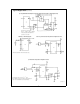
CONTROL INPUTS
[
Note: CLK IN (Pin 4) is the input of a Schmitt trigger circuit and is therefore specified separately
]
V
IN
(1) Logical ‘‘1’’ Input Voltage V
CC
e
5.25 V
DC
2.0 15 V
DC
(Except Pin 4 CLK IN)
2