
User Manual

AC Electrical Characteristics (Continued)
The following specifications apply for V
CC
e
5V
DC
and T
MIN
s
T
A
s
T
MAX
, unless otherwise specified.
Symbol Parameter Conditions Min Typ Max Units
CONTROL INPUTS
[
Note: CLK IN (Pin 4) is the input of a Schmitt trigger circuit and is therefore specified separately
]
V
IN
(0) Logical ‘‘0’’ Input Voltage V
CC
e
4.75 V
DC
0.8 V
DC
(Except Pin 4 CLK IN)
I
IN
(1) Logical ‘‘1’’ Input Current V
IN
e
5V
DC
0.005 1 mA
DC
(All Inputs)
I
IN
(0) Logical ‘‘0’’ Input Current V
IN
e
0V
DC
b
1
b
0.005 mA
DC
(All Inputs)
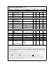
CLOCK IN AND CLOCK R
V
T
a
CLK IN (Pin 4) Positive Going 2.7 3.1 3.5 V
DC
Threshold Voltage
V
T
b
CLK IN (Pin 4) Negative 1.5 1.8 2.1 V
DC
Going Threshold Voltage
V
H
CLK IN (Pin 4) Hysteresis 0.6 1.3 2.0 V
DC
(V
T
a
)
b
(V
T
b
)
V
OUT
(0) Logical ‘‘0’’ CLK R Output I
O
e
360 mA 0.4 V
DC
Voltage V
CC
e
4.75 V
DC
V
OUT
(1) Logical ‘‘1’’ CLK R Output I
O
eb
360 mA 2.4 V
DC
Voltage V
CC
e
4.75 V
DC
DATA OUTPUTS AND INTR
V
OUT
(0) Logical ‘‘0’’ Output Voltage
Data Outputs I
OUT
e
1.6 mA, V
CC
e
4.75 V
DC
0.4 V
DC
INTR Output I
OUT
e
1.0 mA, V
CC
e
4.75 V
DC
0.4 V
DC
V
OUT
(1) Logical ‘‘1’’ Output Voltage I
O
eb
360 mA, V
CC
e
4.75 V
DC
2.4 V
DC
V
OUT
(1) Logical ‘‘1’’ Output Voltage I
O
eb
10 mA, V
CC
e
4.75 V
DC
4.5 V
DC
I
OUT
TRI-STATE Disabled Output V
OUT
e
0V
DC
b
3 mA
DC
Leakage (All Data Buffers) V
OUT
e
5V
DC
3 mA
DC
I
SOURCE
V
OUT
Short to Gnd, T
A
e
25
§
C 4.5 6 mA
DC
I
SINK
V
OUT
Short to V
CC
,T
A
e
25
§
C 9.0 16 mA
DC
POWER SUPPLY
I
CC
Supply Current (Includes f
CLK
e
640 kHz,
Ladder Current) V
REF
/2
e
NC, T
A
e
25
§
C
and CS
e
5V
ADC0801/02/03/04LCJ/05 1.1 1.8 mA
ADC0804LCN/LCV/LCWM 1.9 2.5 mA
Note 1: Absolute Maximum Ratings indicate limits beyond which damage to the device may occur. DC and AC electrical specifications do not apply when operating
the device beyond its specified operating conditions.
Note 2: All voltages are measured with respect to Gnd, unless otherwise specified. The separate A Gnd point should always be wired to the D Gnd.
Note 3: A zener diode exists, internally, from V
CC
to Gnd and has a typical breakdown voltage of 7 V
DC
.
Note 4: For V
IN
(
b
)
t
V
IN
(
a
) the digital output code will be 0000 0000. Two on-chip diodes are tied to each analog input (see block diagram) which will forward
conduct for analog input voltages one diode drop below ground or one diode drop greater than the V
CC
supply. Be careful, during testing at low V
CC
levels (4.5V),
as high level analog inputs (5V) can cause this input diode to conduct–especially at elevated temperatures, and cause errors for analog inputs near full-scale. The
spec allows 50 mV forward bias of either diode. This means that as long as the analog V
IN
does not exceed the supply voltage by more than 50 mV, the output
code will be correct. To achieve an absolute 0 V
DC
to5V
DC
input voltage range will therefore require a minimum supply voltage of 4.950 V
DC
over temperature
variations, initial tolerance and loading.
Note 5: Accuracy is guaranteed at f
CLK
e
640 kHz. At higher clock frequencies accuracy can degrade. For lower clock frequencies, the duty cycle limits can be
extended so long as the minimum clock high time interval or minimum clock low time interval is no less than 275 ns.
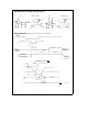
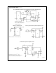
Note 6: With an asynchronous start pulse, up to 8 clock periods may be required before the internal clock phases are proper to start the conversion process. The
start request is internally latched, see
Figure 2
and section 2.0.
Note 7: The CS
input is assumed to bracket the WR strobe input and therefore timing is dependent on the WR pulse width. An arbitrarily wide pulse width will hold
the converter in a reset mode and the start of conversion is initiated by the low to high transition of the WR
pulse (see timing diagrams).
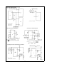
Note 8: None of these A/Ds requires a zero adjust (see section 2.5.1). To obtain zero code at other analog input voltages see section 2.5 and
Figure 5
.
Note 9: The V
REF
/2 pin is the center point of a two-resistor divider connected from V
CC
to ground. In all versions of the ADC0801, ADC0802, ADC0803, and
ADC0805, and in the ADC0804LCJ, each resistor is typically 16 kX. In all versions of the ADC0804 except the ADC0804LCJ, each resistor is typically 2.2 kX.
Note 10: Human body model, 100 pF discharged through a 1.5 kX resistor.
3