
User guide

DS1254
7 of 17
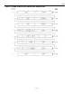
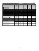
ABSOLUTE MAXIMUM RATINGS*
Voltage Range on Any Pin Relative to Ground -0.3V to +6.0V
Operating Temperature Range 0°C to +70°C
Storage Temperature Range -40°C to +70°C
Soldering Temperature Range See J-STD-020A specification
* This is a stress rating only and functional operation of the device at these or any other conditions
beyond those indicated in the operation sections of this specification is not implied. Exposure to
absolute maximum rating conditions for extended periods of time can affect reliability.
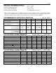
RECOMMENDED DC OPERATING CONDITIONS (0
°
C to +70
°
C)
PARAMETER SYMBOL MIN TYP MAX UNITS
NOTES
Power Supply Voltage
(5V Operation)
V
CC
4.5 5.0 5.5 V 1
Power Supply Voltage
(3.3V Operation)
V
CC
3.0 3.3 3.7 V 1
Logic 1 Voltage All Inputs
V
CC
= 5V±10%
V
CC
= 3.3V±10%
V
IH
V
IH
2.2
2.0
V
CC
+ 0.3
V
CC
+ 0.3
V
V
1
1
Logic 0 Voltage All Inputs
V
CC
= 5V±10%
V
CC
= 3.3V±10%
V
IL
V
IL
-0.3
-0.3
0.8
0.6
V
V
1
1
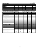
DC ELECTRICAL CHARACTERISTICS (0
°
C to +70
°
C; V
CC
= 5.0V±10%)
PARAMETER SYMBOL MIN TYP MAX UNITS
NOTES
Input Leakage Current I
IL
-4.0 +4.0
µA
I/O Leakage Current I
IO
-4.0 +4.0
µA
Output Current @ 2.4V I
OH
-1.0 mA 3
Output Current @ 0.4V I
OL
2.0 mA 3
Standby Current CE = 2.2V
I
CCS1
5.0 10 mA
Standby Current CE = V
CC
- 0.5V
I
CCS2
3.0 5.0 mA
Operating Current, t
CYC
= 100ns I
CCO1
85 mA
Write Protection Voltage V
PF
4.25 4.50 V 1
DC ELECTRICAL CHARACTERISTICS (0
°
C to +70
°
C; V
CC
= 3.3V±10%)
PARAMETER SYMBOL MIN TYP MAX UNITS
NOTES
Input Leakage Current I
IL
-4.0 +4.0
µA
I/O Leakage Current I
IO
-4.0 +4.0
µA
Output Current @ 2.4V I
OH
-1.0 mA 3
Output Current @ 0.4V I
OL
2.0 mA 3
Standby Current CE = 2.2V
I
CCS1
5.0 7 mA
Standby Current CE = V
CC
- 0.5V
I
CCS2
2.0 3.0 mA
Operating Current, t
CYC
= 100ns I
CCO1
50 mA
Write Protection Voltage V
PF
2.8 2.97 V 1