
User guide


1 of 12 102199
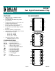
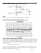
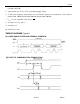
VB
NC
H1
L1
W1
RST
CLK
GND
16
15
14
13
12
11
10
9
1
2
3
4
5
6
7
8
V
CC
NC
S
OUT
W0
H0
L0
C
OUT
DQ
16-Pin SOIC (300-mil)
See Mech. Drawings Section
FEATURES
Ultra-low power consumption, quiet,
pumpless design
Two digitally controlled, 256-position
potentiometers
Serial port provides means for setting and
reading both potentiometers
Resistors can be connected in series to
provide increased total resistance
14-pin DIP, 16-pin SOIC, 20-pin TSSOP
packages
Resistive elements are temperature
compensated to ±0.3 LSB relative linearity
Standard resistance values:
– DS1267-10 ~ 10 kΩ
– DS1267-50 ~ 50 kΩ
– DS1267-100 ~ 100 kΩ
Operating Temperature Range:
– Industrial: -40°C to +85°C
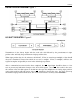
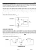
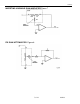
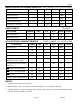
PIN ASSIGNMENT
PIN DESCRIPTIONS
L0, L1 - Low End of Resistor
H0, H1 - High End of Resistor
W0, W1 - Wiper Terminal of Resistor
V
B
- Substrate Bias Voltage
S
OUT
- Stacked Configuration Output
RST - Serial Port Reset Input
DQ - Serial Port Data Input
CLK - Serial Port Clock Input
C
OUT
- Cascade Port Output
V
CC
- +5 Volt Supply
GND - Ground
NC - No Internal Connection
14-Pin DIP (300-mil)
See Mech. Drawings Section
VB
H1
L1
W1
RST
CLK
GND
14
13
12
11
10
9
8
1
2
3
4
5
6
7
V
CC
S
OUT
W0
H0
L0
C
OUT
DQ
DS1267
Dual Digital Potentiometer Chip
www.dalsemi.com
20-Pin TSSOP (173-mil)
VB
NC
H1
L1
W1
RST
CLK
20
19
18
17
16
15
14
1
2
3
4
5
6
7
V
CC
NC
NC
S
OUT
W0
H0
L0
8
9
10
13
12
11
C
OUT
NC
NCNC
GND
DQ