
Owner manual


DS1720
030598 5/12
OPERATION AND CONTROL
The DS1720 must have temperature settings resident in
the TH and TL registers for thermostatic operation. A
configuration/status register is also used to determine
the method of operation that the DS1720 will use in a
particular application, as well as indicating the status of
the temperature conversion operation. The configura-
tion register is defined as follows:
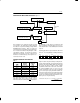
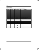
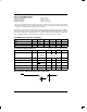
CONFIGURATION/STATUS REGISTER
DONE THF TLF NVB 1 0 CPU 1SHOT
where
DONE = Conversion Done bit. 1=conversion com-
plete, 0=conversion in progress.
THF = Temperature High Flag. This bit will be set
to 1 when the temperature is greater than
or equal to the value of TH. It will remain 1
until reset by writing 0 into this location or
by removing power from the device. This
feature provides a method of determining
if the DS1720 has ever been subjected to
temperatures above TH while power has
been applied.
TLF = Temperature Low Flag. This bit will be set
to 1 when the temperature is less than or
equal to the value of TL. It will remain 1
until reset by writing 0 into this location or
by removing power from the device. This
feature provides a method of determining
if the DS1720 has ever been subjected to
temperatures below TL while power has
been applied.
NVB = Nonvolatile Memory Busy Flag. 1=write to
an E
2
memory cell in progress. 0=nonvol-
atile memory is not busy. A copy to E
2
may take up to 10 ms.
CPU = CPU use bit. If CPU=0, the CLK/CONV
pin acts as a conversion start control,
when RST is low. If CPU is 1, the DS1720
will be used with a CPU communicating to
it over the 3–wire port, and the operation
of the CLK/CONV
pin is as a normal clock
in concert with DQ and RST. This bit is
stored in nonvolatile E
2
memory, capable
of at least 50,000 writes. The DS1720 is
shipped with CPU=0.
1SHOT = One–Shot Mode. If 1SHOT is 1, the
DS1720 will perform one temperature
conversion upon reception of the Start
Convert T protocol. If 1SHOT is 0, the
DS1720 will continuously perform tem-
perature conversion. This bit is stored in
nonvolatile E
2
memory, capable of at least
50,000 writes. The DS1720 is shipped
with 1SHOT=0.
For typical thermostat operation, the DS1720 will oper-
ate in continuous mode. However, for applications
where only one reading is needed at certain times, and
to conserve power, the one–shot mode may be used.
Note that the thermostat outputs (T
HIGH
, T
LOW
, T
COM
)
will remain in the state they were in after the last valid
temperature conversion cycle when operating in one–
shot mode.
OPERATION IN STAND–ALONE MODE
In applications where the DS1720 is used as a simple
thermostat, no CPU is required. Since the temperature
limits are nonvolatile, the DS1720 can be programmed
prior to insertion in the system. In order to facilitate
operation without a CPU, the CLK/CONV
pin (pin 2) can
be used to initiate conversions. Note that the CPU bit
must be set to 0 in the configuration register to use this
mode of operation. Whether CPU=0 or 1, the 3–wire
port is active. Setting CPU=1 disables the stand–alone
mode.
To use the CLK/CONV
pin to initiate conversions, RST
must be low and CLK/CONV must be high. If CLK/
CONV is driven low and then brought high in less than
10 ms, one temperature conversion will be performed
and then the DS1720 will return to an idle state. If CLK/
CONV
is driven low and remains low, continuous con-
versions will take place until CLK/CONV is brought high
again. With the CPU bit set to 0, the CLK/CONV will
override the 1–shot bit if it is equal to 1. This means that
even if the part is set for one–shot mode, driving CLK/
CONV
low will initiate conversions.
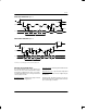
3–WIRE COMMUNICATIONS
The 3–wire bus is comprised of three signals. These are
the RST (reset) signal, the CLK (clock) signal, and the
DQ (data) signal. All data transfers are initiated by driv-
ing the RST
input high. Driving the RST input low termi-
nates communication. (See Figures 4 and 5). A clock
cycle is a sequence of a falling edge followed by a rising
edge. For data inputs, the data must be valid during the
rising edge of a clock cycle. Data bits are output on the