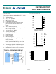
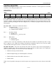
DS17885/DS17887 3V/5V Real-Time Clock www.maxim-ic.com FEATURES PIN ASSIGNMENT Incorporates industry standard DS1287 PC clock plus enhanced features: § Y2K compliant § +3V or +5V operation § SMI recovery stack § 64-bit silicon serial number § Power-control circuitry supports system power-on from date/time alarm or key closure § 32kHz output on power-up § Crystal select bit allows RTC to operate with 6pF or 12.
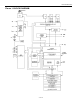
DS17885/DS17887 ORDERING INFORMATION PART # DESCRIPTION DS17885XX-X RTC Chip 3 5 +3V operating range +5V operating range blank commercial temp range N industrial temp range blank 24-pin DIP E 28- pin TSOP S 24- pin SO DS17887X-X RTC Module; 24-pin DIP 3 5 +3V operating rang +5V operating range blank commercial temp range N industrial PIN DESCRIPTION X1 X2 RCLR AD0–AD7 PWR KS CS ALE WR RD IRQ SQW VCC GND VBAT VBAUX NC - Crystal Input Crystal Output RAM Clear Input Multiplexed Address/Data Bus Power-O
DS17885/DS17887 The DS17885/DS17887 power-control circuitry allows the system to be powered on by an external stimulus such as a keyboard or by a time-and-date (wake-up) alarm. The PWR output pin is triggered by one or either of these events, and is used to turn on an external power supply. The PWR pin is under software control, so that when a task is complete, the system power can then be shut down. The DS17885 is a clock/calendar chip with the features described above.
DS17885/DS17887 – RTC Write Input; Active Low. The WR signal is an active low signal. The WR signal defines the time period during which data is written to the addressed register. WR – RTC Chip-Select Input; Active Low. The chip select signal must be asserted low during a bus cycle for DS17885/DS17887 to be accessed. CS must be kept in the active state during RD and WR timing. Bus cycles that take place with ALE asserted but without asserting CS latches addresses. However, no data transfer occurs.
DS17885/DS17887 Figure 1.
DS17885/DS17887 DS17885 ONLY X1, X2 – Connections for a standard 32.768kHz quartz crystal. For greatest accuracy, the DS17885 must be used with a crystal that has a specified load capacitance of either 6pF or 12.5pF. The crystal select (CS) bit in extended-control register 4B is used to select operation with a 6pF or 12.5pF crystal. The crystal is attached directly to the X1 and X2 pins. There is no need for external capacitors or resistors. Note: X1 and X2 are very high-impedance nodes.
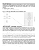
DS17885/DS17887 RTC ADDRESS MAP The address map for the RTC registers of the DS17885/DS17887 is shown in Figure 2. The address map consists of the 14 clock/calendar registers. Ten registers contain the time, calendar, and alarm data, and 4 bytes are used for control and status. All registers can be directly written or read except for the following: 1) Registers C and D are read-only. 2) Bit 7 of Register A is read-only. 3) The high order bit of the second byte is read-only. Figure 2.
DS17885/DS17887 The three time alarm bytes can be used in two ways. First, when the alarm time is written in the appropriate hours, minutes, and seconds alarm locations, the alarm interrupt is initiated at the specified time each day if the alarm enable bit is high. The second use condition is to insert a “don’t care” state in one or more of the three time alarm bytes. The “don’t care” code is any hexadecimal value from C0 to FF.
DS17885/DS17887 CONTROL REGISTERS The four control registers; A, B, C, and D reside in both bank 0 and bank 1. These registers are accessible at all times, even during the update cycle. REGISTER A MSB BIT 7 UIP BIT 6 BIT 5 BIT 4 BIT 3 BIT 2 BIT 1 DV2 DV1 DV0 RS3 RS2 RS1 LSB BIT 0 RS0 UIP – Update-in-Progress. The UIP bit is a status flag that can be monitored. When the UIP bit is a 1, the update transfer occurs soon. When UIP is a 0, the update transfer does not occur for at least 244µs.
DS17885/DS17887 REGISTER B MSB BIT 7 SET BIT 6 BIT 5 BIT 4 BIT 3 BIT 2 BIT 1 LSB BIT 0 PIE AIE UIE SQWE DM 24/12 DSE SET – When the SET bit is a 0, the update transfer functions normally by advancing the counts once per second. When the SET bit is written to a 1, any update transfer is inhibited and the program can initialize the time and calendar bytes without an update occurring in the midst of initializing. Read cycles can be executed in a similar manner.
DS17885/DS17887 REGISTER C MSB BIT 7 BIT 6 BIT 5 BIT 4 BIT 3 BIT 2 BIT 1 PF AF UF 0 0 0 IRQF LSB BIT 0 0 IRQF – Interrupt Request Flag. This bit is set to a 1 when one or more of the following are true: PF = PIE = 1 AF = AIE = 1 UF = UIE = 1 WF = WIE= 1 KF = KSE= 1 RF = RIE = 1 i.e., IRQF = (PF x PIE) + (AF x AIE) + (UF x UIE) + (WF x WIE) + (KF x KSE) + (RF x RIE) Any time the IRQF bit is a 1, the IRQ pin is driven low.
DS17885/DS17887 NV RAM–RTC The general-purpose NV RAM bytes are not dedicated to any special function within the DS17885/DS17887. They can be used by the application program as nonvolatile memory and are fully available during the update cycle. The user RAM is divided into two separate memory banks. When the bank 0 is selected, the 14 real-time clock registers and 114 bytes of user RAM are accessible.
DS17885/DS17887 possible interrupt sources has its flag and enable bits both set. The IRQF bit in Register C is a 1 whenever the IRQ pin is being driven low as a result of one of the six possible active sources. Therefore, determination that the DS17885/DS17887 initiated an interrupt is accomplished by reading Register C and finding IRQF = 1. IRQF remains set until all enabled interrupt flag bits are cleared to 0.
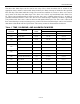
DS17885/DS17887 Table 2. PERIODIC INTERRUPT RATE AND SQUARE-WAVE OUTPUT FREQUENCY EXTENDED REGISTER B SELECT BITS REGISTER A tPI PERIODIC INTERRUPT RATE SQW OUTPUT FREQUENCY E32k RS3 RS2 RS1 RS0 0 0 0 0 0 None None 0 0 0 0 1 3.90625ms 256Hz 0 0 0 1 0 7.8125ms 128Hz 0 0 0 1 1 122.070µs 8.192kHz 0 0 1 0 0 244.141µs 4.096kHz 0 0 1 0 1 488.281µs 2.048kHz 0 0 1 1 0 976.5625µs 1.024kHz 0 0 1 1 1 1.953125ms 512Hz 0 1 0 0 0 3.
DS17885/DS17887 UPDATE CYCLE The serialized RTC executes an update cycle once per second regardless of the SET bit in Register B. When the SET bit in Register B is set to 1, the user copy of the double-buffered time, calendar, alarm, and elapsed time byte is frozen and does not update as the time increments. However, the time countdown chain continues to update the internal copy of the buffer.
DS17885/DS17887 EXTENDED FUNCTIONS The extended functions provided by the DS17885/DS17887 that are new to the RAMified RTC family are accessed by a software-controlled bank-switching scheme, as illustrated in Figure 4. In bank 0, the clock/calendar registers and 50 bytes of user RAM are in the same locations as for the DS1287. As a result, existing routines implemented within BIOS, DOS, or application software packages can gain access to the DS17885/DS17887 clock registers with no changes.
DS17885/DS17887 can be used to determine if and how many RTC writes have occurred since the last time this register was read. Auxiliary Battery The VBAUX input is provided to supply power from an auxiliary battery for the DS17885/DS17887 kickstart, wake-up, and SQW output features in the absence of VCC. This power source must be available in order to use these auxiliary features when no VCC is applied to the device.
DS17885/DS17887 A kickstart sequence occurs when kickstarting is enabled through KSE = 1. While the system is powered down, the KS input pin is monitored for a low-going transition of minimum pulse width tKSPW. When such a transition is detected, the PWR line is pulled low, as it is for a wake-up condition. Also at this time, the kickstart Flag (KF, bank 1, register 04AH) is set, indicating that a kickstart condition has occurred.
DS17885/DS17887 During interval 5, the system is fully powered down. Battery backup of the clock calendar and NV RAM is in effect and IRQ is tri-stated, and monitoring of wake-up and kickstart takes place. If PRS = 1, PWR stays active; otherwise, if PRS = 0 PWR is tri-stated. RAM Clear The DS17885/DS17887 provides a RAM clear function for the 114 bytes of user RAM. When enabled, this function can be performed regardless of the condition of the VCC pin.
DS17885/DS17887 Figure 4.
DS17885/DS17887 EXTENDED CONTROL REGISTERS Two extended control registers are provided to supply controls and status information for the extended features offered by the DS17885/DS17887. These are designated as extended control registers 4A and 4B and are located in register bank 1, locations 04AH and 04BH, respectively. The functions of the bits within these registers are described as follows.
DS17885/DS17887 EXTENDED CONTROL REGISTER 4B MSB BIT 7 BIT 6 BIT 5 BIT 4 BIT 3 BIT 2 BIT 1 LSB BIT 0 ABE E32k CS RCE PRS RIE WIE KSE ABE – Auxiliary Battery Enable. This bit when written to a logic 1 enables the VBAUX pin for extended functions. E32k – Enable 32.768kHz Output. This bit when written to a logic 1 enables the 32.768kHz oscillator frequency to be output on the SQW pin. E32k is set to a 1 when VCC is powered up. CS – Crystal Select.
DS17885/DS17887 SYSTEM MAINTENANCE INTERRUPT (SMI) RECOVERY STACK An SMI recovery register stack is located in the extended register bank, locations 4Eh and 4Fh. This register stack, shown below, can be used by the BIOS to recover from an SMI occurring during an RTC read or write. The RTC address is latched on the falling edge of the ALE signal. Each time an RTC address is latched, the register address stack is pushed.
DS17885/DS17887 ABSOLUTE MAXIMUM RATINGS* Voltage Range on Any Pin Relative to Ground Storage Temperature Range Soldering Temperature Range -0.3V to +7.0V -40°C to +85°C +260°C for 10 seconds (DIP) (Note 13) See IPC/JEDEC Standard J-STD-020A for Surface Mount Devices * This is a stress rating only and functional operation of the device at these or any other conditions beyond those indicated in the operation sections of this specification is not implied.
DS17885/DS17887 DC ELECTRICAL CHARACTERISTICS PARAMETER SYMBOL Over the operating range (5V) MIN TYP MAX UNITS NOTES Average VCC Power Supply Current ICC1 25 50 mA 1, 2 CMOS Standby Current ( CS = VCC - 0.2V) ICC2 1 3 mA 1, 2 Input Leakage Current (Any Input) IIL -1 +1 mA Output Leakage Current IOL -1 +1 mA Output Logic 1 Voltage (IOUT = -1.0mA) VOH 2.4 Output Logic 0 Voltage (IOUT = +2.
DS17885/DS17887 DC ELECTRICAL CHARACTERISTICS PARAMETER SYMBOL Over the operating range (3V) MIN TYP MAX UNITS NOTES Average VCC Power-Supply Current ICC1 15 30 mA 1, 2 CMOS Standby Current ( CS = VCC - 0.2V) ICC2 0.5 2 mA 1, 2 Input Leakage Current (Any Input) IIL -1 +1 mA Output Leakage Current IOL -1 +1 mA Output Logic 1 Voltage at -0.4mA VOH 2.4 Output Logic 0 Voltage at +0.
DS17885/DS17887 RTC AC TIMING CHARACTERISTICS PARAMETER Over the operating range (3V) SYMBOL MIN tCYC 360 Pulse-Width, RD / WR Low PWRWL 200 ns Pulse-Width, RD / WR High PWRWH 150 ns Cycle Time Input Rise and Fall tR , t F TYP MAX UNITS DC ns 30 ns Chip-Select Setup Time Before WR or RD tCS 20 ns Chip-Select Hold Time tCH 0 ns Read Data Hold Time tDHR 10 Write Data Hold Time tDHW 0 ns Muxed Address Valid Time to ALE Fall tASL 40 ns Muxed Address Hold Time to ALE F
DS17885/DS17887 RTC AC TIMING CHARACTERISTICS PARAMETER Over the operating range (5V) SYMBOL MIN tCYC 240 Pulse-Width, RD / WR Low PWRWL 120 ns Pulse-Width, RD / WR High PWRWH 80 ns Cycle Time TYP MAX UNITS DC ns Input Rise and Fall Time tR, tF Chip-Select Setup Time before WR or RD tCS 20 ns Chip-Select Hold Time tCH 0 ns Read Data Hold Time tDHR 10 Write Data Hold Time tDHW 0 ns Muxed Address Valid Time to ALE Fall tASL 20 ns Muxed Address Hold Time to ALE fall t
DS17885/DS17887 BUS TIMING FOR READ CYCLE TO RTC AND RTC REGISTERS BUS TIMING FOR WRITE CYCLE TO RTC AND RTC REGISTERS 29 of 38
DS17885/DS17887 POWER-UP/POWER-DOWN TIMING, 5V PARAMETER SYMBOL High to Power-Fail tPF Recovery at Power-Up tREC CS VCC Slew Rate Power-Down VCC Slew Rate Power-Down VCC Slew Rate Power-Up Expected Data Retention (TA = +25°C) MIN TYP MAX UNITS 0 ns 150 tF 4.0 £ VCC £ 4.5V tFB 3.0 £ VCC £ 4.0V ms 10 ms 0 ms 10 years 4.5 ³ VCC ³ 4.
DS17885/DS17887 POWER-UP CONDITION, 3V POWER-DOWN CONDITION, 3V 31 of 38
DS17885/DS17887 POWER-UP CONDITION, 5V POWER-DOWN CONDITION, 5V 32 of 38
DS17885/DS17887 WAKE-UP/KICKSTART TIMING Note: Time intervals shown above are referenced in Wake-Up/Kickstart section. *This condition can occur with the 3V device.
DS17885/DS17887 BURST MODE TIMING WAVEFORM NOTES: 1) 2) 3) 4) 5) 6) 7) Typical values are at +25°C and nominal supplies. Outputs are open. Write-protection trip point occurs during power-fail prior to switchover from VCC to VBAT. Applies to the AD0 to AD7 pins, and the SQW pin when each is in a high-impedance state. The IRQ and PWR pins are open-drain. Measured with a load of 50pF + 1 TTL gate. Wake-up kickstart timeout generated only when the oscillator is enabled and the countdown chain is not reset.
DS17885/DS17887 DS17885 24-PIN DIP PKG DIM A IN MM B IN MM C IN MM D IN MM E IN MM F IN MM G IN MM H IN MM J IN MM K IN MM 24-PIN MIN MAX 1.245 1.270 31.62 32.25 0.530 0.550 13.46 13.97 0.140 0.160 3.56 4.06 0.600 0.625 15.24 15.88 0.015 0.050 0.380 1.27 0.120 0.145 3.05 3.68 0.090 0.110 2.29 2.79 0.625 0.675 15.88 17.15 0.008 0.012 0.20 0.30 0.015 0.022 0.38 0.
DS17885/DS17887 DS17885 24-PIN SO The chamfer on the body is optional. If it is not present, a terminal 1 identifier must be positioned so that one-half or more of its area is contained in the hatched zone. PKG DIM A IN MM A1 IN MM A2 IN MM b IN MM C IN MM D IN MM e IN MM E1 IN MM H IN MM L IN MM Θ 24-PIN MIN MAX 0.094 0.105 2.38 2.68 0.004 0.012 0.102 0.30 0.089 0.095 2.26 2.41 0.013 0.020 0.33 0.51 0.009 0.013 0.229 0.33 0.598 0.612 15.19 15.54 0.050 BSC 1.27 BSC 0.290 0.300 7.37 7.62 0.398 0.416 10.
DS17885/DS17887 DS17885 28-PIN TSOP PKG DIM A A1 A2 b c D D1 E e L L1 28-PIN MIN MAX — 1.20 0.05 — 0.91 1.02 0.18 0.27 0.15 0.20 13.20 13.60 11.70 11.90 7.90 8.10 0.55 BSC 0.30 0.70 0.
DS17885/DS17887 DS17887 RTC PLUS RAM Note: Pins 2, 3, 16, and 20 are missing by design. PKG DIM A IN MM B IN MM C IN MM D IN MM E IN MM F IN MM G IN MM H IN MM J IN MM K IN MM 24-PIN MIN MAX 1.320 1.335 33.53 33.91 0.720 0.740 18.29 18.80 0.345 0.370 8.76 9.40 0.100 0.130 2.54 3.30 0.015 0.030 0.38 0.76 0.100 0.140 2.79 3.56 0.090 0.110 2.29 2.79 0.590 0.630 14.99 16.00 0.008 0.012 0.20 0.30 0.015 0.021 0.38 0.