
Manual

DS1857
Dual Temperature-Controlled Resistors with
External Temperature Input and Monitors
______________________________________________ Maxim Integrated Products 1
For pricing delivery, and ordering information please contact Maxim/Dallas Direct! at
1-888-629-4642, or visit Maxim’s website at www.maxim-ic.com.
General Description
The DS1857 dual temperature-controlled nonvolatile
(NV) variable resistors with external temperature input
and monitors consists of two 50kΩ 256-position linear
variable resistors, two analog monitor inputs (MON1,
MON2), and an external temperature sensor input. The
device provides an ideal method for setting and tem-
perature-compensating bias voltages and currents in
control applications using minimal circuitry. The vari-
able resistor settings are stored in EEPROM memory
and can be accessed over the 2-wire serial bus.
Applications
Optical Transceivers
Optical Transponders
Instrumentation and Industrial Controls
RF Power Amps
Diagnostic Monitoring
Features
♦ Four Total Monitored Channels (Temperature,
V
CC
, MON1, MON2)
♦ Two External Analog Inputs (MON1, MON2)
♦ Interface to External Temperature Sensor (LM50)
♦ Two 50kΩ, Linear, 256-Position, Nonvolatile
Temperature-Controlled Variable Resistors
♦ Resistor Settings Changeable Every 2°C
♦ Access to Monitoring and ID Information
Configurable with Separate Device Addresses
♦ Resistor Disable (Open-Circuit) Function
♦ 2-Wire Serial Interface
♦ Three Address Lines for Multiple Devices
♦ Operates from a 3.3V or 5V Supply
♦ SFF-8472 Compatible
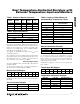
Ordering Information
Rev 0; 1/03
PART
TEMP RANGE
PIN-PACKAGE
DS1857E-050
-40°C to +95°C
16 TSSOP
DS1857E-050/T&R
-40°C to +95°C
16 TSSOP
(Tape-and-Reel)
DS1857B-050
-40°C to +95°C
16 Ball CSBGA
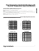
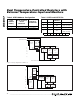
A
TOP VIEW
B
C
D
1
16-BALL CSBGA (4mm x 4mm)
1.0mm PITCH
16 TSSOP
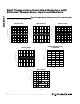
324
EXTTMP
A0WPENRHIZ
MON2MON1L0GND
H1V
CC
SCLA1
L1H0SDAA2
DS1857
SDA
1
2
3
4
5
6
7
8
16
15
14
13
12
11
10
9
SCL
A0
A1
A2
WPEN
RHIZ
GND
V
CC
H1
L1
H0
L0
EXTTMP
MON2
MON1
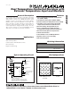
Pin Configurations
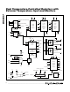
DS1857
SDA
1
2
3
4
5
6
7
8
16
0.1µF
15
14
13
12
11
10
9
SCL
A0**
A1**
A2**
WPEN
RHIZ
GND
V
CC
H1
L1
H0
L0
EXTTMP
MON2
MON1
Tx DISABLE
TO EXTERNAL TEMPERATURE
SENSOR, SUCH AS LM50
DIAGNOSTIC
INPUTS
0 TO 2.5V FS
TO LASER BIAS
CONTROL
TO LASER MODULATION
CONTROL
DECOUPLING
CAP
Rx POWER*
Tx BIAS*
*Rx POWER AND Tx BIAS CAN BE ARBITRARILY
ASSIGNED TO THE MON INPUTS.
**ADDRESS INPUTS DETERMINE THE MAIN DEVICE 2-WIRE
SLAVE ADDRESS WHEN ADFIX = 0. THIS ADDRESS MUST BE
DIFFERENT THAN THE AUX DEVICE ADDRESS WHEN ADEN = 0.
V
CC
V
CC
V
CC
= 3.3V
4.7kΩ4.7kΩ
2-WIRE
INTERFACE
GROUND TO
DISABLE WRITE
PROTECT
Typical Operating Circuit