Rev 1; 10/08 PON Triplexer and SFP Controller The DS1875 controls and monitors all functions for burstmode transmitters, APD receivers, and video receivers. It also includes a power-supply controller for APD bias generation, and provides all SFF-8472 diagnostic and monitoring functionality. The combined solution of the DS1875 and the MAX3643 laser driver provides APC loop, modulation current control, and eye safety functionality.
DS1875 PON Triplexer and SFP Controller TABLE OF CONTENTS Absolute Maximum Ratings . . . . . . . . . . . . . . . . . . . . . . . . . . . . . . . . . . . . . . . . . . . . . . . . . . . . . . . . . . . . . . . . . . . . . .5 Recommended Operating Conditions . . . . . . . . . . . . . . . . . . . . . . . . . . . . . . . . . . . . . . . . . . . . . . . . . . . . . . . . . . . . . .5 AC Electrical Characteristics . . . . . . . . . . . . . . . . . . . . . . . . . . . . . . . . . . . . . . . . . . . . . . . . . .
PON Triplexer and SFP Controller Die Identification . . . . . . . . . . . . . . . . . . . . . . . . . . . . . . . . . . . . . . . . . . . . . . . . . . . . . . . . . . . . . . . . . . . . . . . . . . .23 Low-Voltage Operation . . . . . . . . . . . . . . . . . . . . . . . . . . . . . . . . . . . . . . . . . . . . . . . . . . . . . . . . . . . . . . . . . . . . . .23 Enhanced RSSI Monitoring (Dual Range Functionality) . . . . . . . . . . . . . . . . . . . . . . . . . . . . . . . . . . . . . . . . . . . . .
DS1875 PON Triplexer and SFP Controller TABLE OF CONTENTS (continued) Auxiliary Memory A0h Register Descriptions . . . . . . . . . . . . . . . . . . . . . . . . . . . . . . . . . . . . . . . . . . . . . . . . . . . . .91 Package Information . . . . . . . . . . . . . . . . . . . . . . . . . . . . . . . . . . . . . . . . . . . . . . . . . . . . . . . . . . . . . . . . . . . . . . . . . .91 LIST OF FIGURES Figure 1. Power-Up Timing (BEN is a Long Burst) . . . . . . . . . . . . . . . . . . . . . . . . . . . .
PON Triplexer and SFP Controller Operating Temperature Range ...........................-40°C to +95°C Programming Temperature Range .........................0°C to +85°C Storage Temperature Range .............................-55°C to +125°C Soldering Temperature...........................Refer to the IPC/JEDEC J-STD-020 Specification. *Subject to not exceeding +6V. Stresses beyond those listed under “Absolute Maximum Ratings” may cause permanent damage to the device.
DS1875 PON Triplexer and SFP Controller ELECTRICAL CHARACTERISTICS (DAC1 AND M4DAC) (VCC = +2.85V to +3.9V, TA = -40°C to +95°C, unless otherwise noted.) PARAMETER SYMBOL CONDITIONS MIN DAC Output Range DAC Output Resolution TYP MAX UNITS 2.5 V 8 Bits DAC Output Integral Nonlinearity -1 +1 LSB DAC Output Differential Nonlinearity -1 +1 LSB DAC Error -1.25 +1.
PON Triplexer and SFP Controller (VCC = +2.85V to +3.9V, TA = -40°C to +95°C, unless otherwise noted.) PARAMETER PWM-DAC Full-Scale Voltage SYMBOL CONDITIONS MIN VPWM-DAC TYP PWM-DAC Resolution VPWM-DAC Full-Scale Voltage Error MAX UNITS 8 Bits 1.25 TA = +25°C V 1.
DS1875 PON Triplexer and SFP Controller ANALOG VOLTAGE MONITORING (VCC = +2.85V to +3.9V, TA = -40°C to +95°C, unless otherwise noted.) PARAMETER SYMBOL CONDITIONS MIN ADC Resolution MAX 13 Input/Supply Accuracy (MON1–MON8, VCC) ACC Update Rate for Temp, MON1–MON4, and VCC tFRAME:1 Update Rate for MON5–MON8 tFRAME:2 Input/Supply Offset (MON1–MON8, VCC) VOS At factory setting Bit EN5TO8B is enabled in Table 02h, Register 89h (Note 11) MON1–MON8 Factory Setting TYP Bits 0.25 0.
PON Triplexer and SFP Controller (VCC = +2.85V to +3.9V, TA = -40°C to +95°C, timing referenced to VIL(MAX) and VIH(MIN).) (See Figure 15.) PARAMETER SYMBOL CONDITIONS (Note 12) MIN 0 TYP MAX UNITS 400 kHz SCL Clock Frequency f SCL Clock Pulse-Width Low tLOW 1.3 μs Clock Pulse-Width High tHIGH 0.6 μs Bus-Free Time Between STOP and START Condition tBUF 1.3 μs START Hold Time tHD:STA 0.6 μs START Setup Time t SU:STA 0.
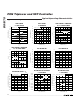
Typical Operating Characteristics (VCC = +2.85V to +3.9V, TA = +25°C, unless otherwise noted.) SUPPLY CURRENT vs. SUPPLY VOLTAGE +95°C +25°C 6.5 6.0 5.5 7.4 7.3 7.2 VCC = 3.9V 8.0 7.1 7.5 ICC (mA) SUPPLY CURRENT (mA) 7.0 VCC = 2.85V 6.5 6.7 6.6 5.0 5.0 6.5 4.5 4.5 6.4 3.35 3.85 -40 -20 0 VCC (V) 8.0 SW = 131.25kHz 7.6 7.4 0 20 40 60 60 80 0.8 0.4 0.2 0 -0.2 -0.4 0.6 0.4 0.2 0 -0.2 -0.4 -0.6 -0.6 -0.8 -0.8 -1.
PON Triplexer and SFP Controller 40 30 70 CALCULATED VALUE 60 50 40 30 0.2 0 -0.2 -0.4 20 -0.6 10 10 -0.8 0 0 -1.0 000 001 002 003 004 005 006 007 000 001 010 011 100 101 110 111 MOD RANGING VALUE (DEC) COMP RANGING (DEC) 0 -0.2 0.4 0.8 0.6 0.2 0 -0.2 0.4 0.2 0 -0.2 -0.4 -0.4 -0.4 -0.6 -0.6 -0.6 -0.8 -0.8 -0.8 -1.0 -1.0 -1.0 0.5 1.0 1.5 2.5 2.0 0 50 100 150 MON1 TO MON8 INPUT VOLTAGE (V) APC INDEX (DEC) FB VOLTAGE vs. TEMPERATURE PWM DAC = FFh VOUT vs.
Typical Operating Characteristics (continued) (VCC = +2.85V to +3.9V, TA = +25°C, unless otherwise noted.) PWM DAC INL 0.75 0.75 0.25 0 -0.25 0.50 DAC DNL (LSB) 0.50 DAC INL (LSB) 0.50 1.00 DS1875 toc20 DS1875 toc19 0.75 M3QT DAC DNL 1.00 0.25 0 -0.25 0.25 0 -0.25 -0.50 -0.50 -0.50 -0.75 -0.75 -0.75 -1.00 -1.00 0 32 64 96 128 160 192 224 256 -1.
PON Triplexer and SFP Controller PIN NAME 1 BEN Burst-Enable Input. Triggers the samples for the APC and quick-trip monitors. FUNCTION 2 SDA I2C Serial-Data Input/Output 3 SCL I2C Serial-Clock Input 4 TX-F Transmit-Fault Output 5, 7, 11, 20, 36, 37, 38 N.C. No Connection 6 FETG FET Gate Output. Signals an external n-channel or p-channel MOSFET to enable/disable the laser’s current. Transmit-Disable Input. Disables analog outputs. 8 TX-D 9, 31, 35 VCC Power-Supply Input (2.85V to 3.
PON Triplexer and SFP Controller DS1875 Block Diagram DS1865 MEMORY ORGANIZATION VCC VCC SDA SCL MAIN MEMORY EEPROM/SRAM ADC CONFIGURATION/RESULTS TABLE 00h (EEPROM) SYSTEM STATUS BITS ADDITIONAL MONITORS ALARM/WARNING COMPARISONS I2C INTERFACE EEPROM 256 BYTES AT A0h SLAVE ADDRESS VCC TABLE 01h (EEPROM) USER MEMORY, ALARM TRAP TABLE 05h (EEPROM) ADC TE LUT TABLE 02h (EEPROM) CONFIGURATION AND CALIBRATION TABLE 06h (EEPROM) M4DAC LUT TABLE 03h (EEPROM) USER MEMORY TABLE 07h (EEPROM) PWM LUT TABL
PON Triplexer and SFP Controller 3.3V IN+ VCC IN- OUT+ BEN+ OUT- BEN- BIASMAX3643 DIS BCMON BENOUT BIASSET VBSET VREF MODSET IMAX VMSET GND BIAS+ MAX4003 RF DETECTOR 12V MOD I2C COMMUNICATION BIAS BEN SDA BMD SCL MON1 FAULT OUTPUT TX-F MON2 TRANSMIT POWER DISABLE INPUT TX-D MON3 RECEIVER LOS LOSI MON4 RECEIVE POWER CATV RF POWER OPEN-DRAIN LOS OUTPUT CATV FETG D0 GAIN CONTROL M4DAC ADDITIONAL DIGITAL I/O MAX3654 FTTH CATV TIA D3 D1 CATV SHUTDOWN CONTROL 3.
DS1875 PON Triplexer and SFP Controller Detailed Description The DS1875 integrates the control and monitoring functionality required to implement a PON system using Maxim’s MAX3643 compact burst-mode laser driver. The compact laser-driver solution offers a considerable cost benefit by integrating control and monitoring features in the low-power CMOS process, while leaving only the high-speed portions to the laser driver.
PON Triplexer and SFP Controller BIAS and MOD Output During Power-Up On power-up the modulation and bias outputs remain off until VCC is above VPOA, a temperature conversion has been completed, and, if the VCC ADC alarm is enabled, a VCC conversion above the customer-defined VCC low alarm level must clear the VCC low alarm (tINIT). Once all these conditions (tINIT) are satisfied, the MOD output is enabled with the value determined by the temperature conversion and the modulation LUT (Table 04h).
DS1875 PON Triplexer and SFP Controller BIAS and MOD Output as a Function of Transmit Disable (TX-D) If the TX-D pin is asserted (logic 1) during normal operation, the outputs are disabled within tOFF. When TX-D is deasserted (logic 0), the DS1875 turns on the MOD output with the value associated with the present temperature and initializes the BIAS using the same search algorithm used at startup.
PON Triplexer and SFP Controller Monitors and Fault Detection Monitors Monitoring functions on the DS1875 include a power-on analog (POA) VCC comparison, five quick-trip comparators, and ADC channels. This monitoring combined with the interrupt masks determine if the DS1875 shuts down its outputs and triggers the TX-F and FETG outputs. All the monitoring levels and interrupt masks are user programmable with the exception of POA, which trips at a fixed range and is nonmaskable for safety reasons.
DS1875 PON Triplexer and SFP Controller TRIP CONDITION mCLK (525kHz) CAPTURE ALARM M3QT ALARM (UNLATCHED) Figure 4. M3QT Timing ONE ADC CYCLE MON4 TEMP VCC MON1 MON2 MON3 MON4 TEMP tFRAME1 Figure 5. ADC Timing with EN5TO8B = 0 TEMP VCC MON1 MON2 MON3 MON4 MON5 MON6 tFRAME2 TEMP VCC MON1 MON2 MON3 MON4 MON7 MON8 tFRAME2 Figure 6.
PON Triplexer and SFP Controller 62h–6Bh). This is true during the setup of internal calibration as well as during subsequent data conversions. Transmit Fault (TX-F) Output The TX-F output has masking registers for the ADC alarms and the QT alarms to select which comparisons cause it to assert. In addition, the FETG alarm is selectable through the TX-F mask to cause TX-F to assert. All alarms, with the exception of FETG, only cause TX-F to remain active while the alarm condition persists.
DS1875 PON Triplexer and SFP Controller DETECTION OF FETG FAULT TX-D IBIAS VMOD FETG* tOFF tON tOFF tON tFETG:ON tFETG:OFF *FETG DIR = 0 Figure 8. FETG/Output Disable Timing (Fault Condition Detected) Safety Shutdown (FETG) Output The FETG output has masking registers (separate from TX-F) for the ADC alarms and the QT alarms to select which comparisons cause it to assert. Unlike TX-F, the FETG output is always latched.
PON Triplexer and SFP Controller Low-Voltage Operation The DS1875 contains two power-on reset (POR) levels. The lower level is a digital POR (VPOD) and the higher level is an analog POR (VPOA). At startup, before the supply voltage rises above VPOA, the outputs are disabled (FETG and BIAS outputs are high impedance, MOD is low), all SRAM locations are low (including shadowed EEPROM (SEE)), and all analog circuitry is disabled.
DS1875 PON Triplexer and SFP Controller Dual-range functionality consists of two modes of operation: fine mode and coarse mode. Each mode is calibrated for a unique transfer function, hence the term, dual range. Table 6 highlights the registers related to MON3. Fine mode is equivalent to the other MON channels. Fine mode is calibrated using the gain, offset, and right-shifting registers at locations shown in Table 6 and is ideal for relatively small analog input voltages.
PON Triplexer and SFP Controller NO. OF RIGHTSHIFTS FINE MODE (MAX) COARSE MODE (MIN*) 0 FFF8h F000h 1 7FFCh 7800h 2 3FFEh 3C00h 3 1FFFh 1E00h 4 0FFFh 0F00h 5 07FFh 0780h 6 03FFh 03C0h 7 01FFh 01E0h *This is the minimum reported coarse-mode conversion. two thresholds. The actual threshold values are a function of the number of right-shifts being used. Table 7 shows the threshold values for each possible number of right-shifts.
DS1875 PON Triplexer and SFP Controller than the PWM DAC level, the error amplifier increases the level on the COMP pin. The level on the COMP pin is compared to the signal from the oscillator and ramp generator to set the duty cycle that is input to the gate driver and maximum duty-cycle limiting block. An increase on the COMP pin increases the duty cycle. Conversely, if FB is greater than the PWM DAC, the level on COMP is decreased, decreasing the duty cycle.
PON Triplexer and SFP Controller POLE1 (dominant pole) = 1/(2π × REA × CCOMP) ZERO1 (compensation zero) = 1/(2π × RCOMP × CCOMP) POLE2 (output load pole) = 2 × VOUT − VIN 1 × VOUT − VIN 2π × R LOAD × ( C2 + C3 ) POLE3 (output filter pole) = 1/(2π × R1 × C3) The DC open-loop gain is given by: AOL = GM × R EA × ⎛V − VIN R LOAD × T ⎞ 2 × VIN VFB × × ⎜ OUT × ⎟ 0.
DS1875 PON Triplexer and SFP Controller VIN D1 L1 C1 R1 C2 VOUT C3 R2 SW R4 3.3V Q1 R3 MAX4007 FB RCOMP CCOMP RMON COMP C4 DS1875 D2 APD OVERLOAD QUICK TRIP ROSA APD TIA MON3 Figure 12. PWM Controller Typical APD Bias Circuit CURRENT SINK VOLTAGE OUTPUT SW SW DS1875 FB COMP Figure 13. PWM Controller Voltage Output Configuration 28 DS1875 FB COMP Figure 14.
PON Triplexer and SFP Controller DS1875 SDA tBUF tF tHD:STA tLOW tSP SCL tHIGH tHD:STA tHD:DAT STOP tSU:STA tR tSU:STO tSU:DAT START REPEATED START NOTE: TIMING IS REFERENCED TO VIL(MAX) AND VIH(MIN). Figure 15. I2C Timing Diagram I2C Communication I2C Definitions The following terminology is commonly used to describe I2C data transfers. Master Device: The master device controls the slave devices on the bus. The master device generates SCL clock pulses and START and STOP conditions.
PON Triplexer and SFP Controller DS1875 Byte Write: A byte write consists of 8 bits of information transferred from the master to the slave (most significant bit first) plus a 1-bit acknowledgement from the slave to the master. The 8 bits transmitted by the master are done according to the bit write definition and the acknowledgement is read using the bit read definition.
PON Triplexer and SFP Controller Memory Map Memory Organization The DS1875 features 10 separate memory tables that are internally organized into 8-byte rows. The Lower Memory is addressed from 00h to 7Fh and contains alarm and warning thresholds, flags, masks, several control registers, password entry area (PWE), and the table select byte. Table 00h contains conversion results for MON5 through MON8.
DS1875 PON Triplexer and SFP Controller DEC HEX 0 0h I2C SLAVE ADDRESS A0h (FIXED) I2C SLAVE ADDRESS A2h (DEFAULT) 00h 00h LOWER MEMORY AUXILIARY MEMORY DIGITAL DIAGNOSTIC FUNCTIONS 2Fh 30h PW2 LEVEL ACCESS EEPROM (48 BYTES) 5Fh 60h DIGITAL DIAGNOSTIC FUNCTIONS 7Ah PASSWORD ENTRY (PWE) (7Bh–Eh) TABLE SELECT BYTE 7Fh EEPROM DEC HEX 128 80h 80h MON5–MON8 CONV 80h 80h 80h 80h 80h 80h 80h 80h 88h 89h TABLE 01h TABLE 02h TABLE 03h TABLE 04h TABLE 05h TABLE 06h TABLE 07h TABLE 08h P
PON Triplexer and SFP Controller Lower Memory Register Map This register map shows each byte/word (2 bytes) in terms of the row it is on in the memory. The first byte in the row is located in memory at the row address (hexadecimal) in the leftmost column. Each subsequent byte on the row is one/two memory locations beyond the previous byte/word’s address. A total of 8 bytes are present on each row. For more information about each of these bytes, see the corresponding register description.
DS1875 PON Triplexer and SFP Controller Table 00h Register Map TABLE 00h ROW (HEX) ROW NAME 80 <2>ADC VALUES2 88–FF EMPTY ACCESS CODE Read Access Write Access 34 <0> See each bit/byte separately WORD 0 BYTE 0/8 WORD 1 BYTE 1/9 BYTE 2/A MON5 VALUE EMPTY BYTE 3/B WORD 2 BYTE 4/C MON6 VALUE EMPTY EMPTY WORD 3 BYTE 5/D BYTE 6/E MON7 VALUE EMPTY EMPTY EMPTY BYTE 7/F MON8 VALUE EMPTY EMPTY <1> <2> <3> <4> <5> <6> <7> <8> <9> <10> <11> All All All PW2 All N/A PW1 PW
PON Triplexer and SFP Controller TABLE 01h (PW1) WORD 0 WORD 1 WORD 2 WORD 3 ROW (HEX) ROW NAME BYTE 0/8 BYTE 1/9 BYTE 2/A BYTE 3/B BYTE 4/C BYTE 5/D BYTE 6/E BYTE 7/F 80 <7>PW1 EE EE EE EE EE EE EE EE EE 88 <7>PW1 EE EE EE EE EE EE EE EE EE 90 <7>PW1 EE EE EE EE EE EE EE EE EE 98 <7>PW1 EE EE EE EE EE EE EE EE EE A0 <7>PW1 EE EE EE EE EE EE EE EE EE A8 <7>PW1 EE EE EE EE EE EE EE EE EE B0 <7>PW1 EE EE EE EE EE EE EE EE EE B
DS1875 PON Triplexer and SFP Controller Table 02h Register Map TABLE 02h (PW2) ROW (HEX) ROW NAME WORD 0 BYTE 0/8 WORD 1 BYTE 1/9 BYTE 2/A WORD 2 BYTE 3/B BYTE 4/C BYTE 7/F <10>DEVICE <10>DEVICE <0>CONFIG0 <8>MODE 88 <8>CONFIG1 SAMPLE RATE 90 <8>SCALE0 RESERVED VCC SCALE MON1 SCALE MON2 SCALE 98 <8>SCALE1 MON3 FINE SCALE MON4 SCALE MON3 COARSE SCALE RESERVED A0 <8>OFFSET0 RESERVED VCC OFFSET MON1 OFFSET MON2 OFFSET MON4 OFFSET MON3 COARSE OFFSET INTERNAL TEMP OFFSET* PW
PON Triplexer and SFP Controller TABLE 03h (PW2) WORD 0 WORD 1 WORD 2 WORD 3 ROW (HEX) ROW NAME BYTE 0/8 BYTE 1/9 BYTE 2/A BYTE 3/B BYTE 4/C BYTE 5/D BYTE 6/E BYTE 7/F 80 <8>PW2 EE EE EE EE EE EE EE EE EE 88 <8>PW2 EE EE EE EE EE EE EE EE EE 90 <8>PW2 EE EE EE EE EE EE EE EE EE 98 <8>PW2 EE EE EE EE EE EE EE EE EE A0 <8>PW2 EE EE EE EE EE EE EE EE EE A8 <8>PW2 EE EE EE EE EE EE EE EE EE B0 <8>PW2 EE EE EE EE EE EE EE EE EE B
DS1875 PON Triplexer and SFP Controller Table 04h Register Map TABLE 04h (MODULATION LUT) WORD 0 WORD 1 WORD 2 WORD 3 ROW (HEX) ROW NAME BYTE 0/8 BYTE 1/9 BYTE 2/A BYTE 3/B BYTE 4/C BYTE 5/D BYTE 6/E BYTE 7/F 80 <8>LUT4 MOD MOD MOD MOD MOD MOD MOD MOD 88 <8>LUT4 MOD MOD MOD MOD MOD MOD MOD MOD 90 <8>LUT4 MOD MOD MOD MOD MOD MOD MOD MOD 98 <8>LUT4 MOD MOD MOD MOD MOD MOD MOD MOD A0 <8>LUT4 MOD MOD MOD MOD MOD MOD MOD MOD A8 <8>LUT4 MOD MOD
PON Triplexer and SFP Controller TABLE 06h (M4DAC LUT) WORD 0 WORD 1 WORD 2 WORD 3 ROW (HEX) ROW NAME BYTE 0/8 BYTE 1/9 BYTE 2/A BYTE 3/B BYTE 4/C BYTE 5/D BYTE 6/E BYTE 7/F 80 <8>LUT6 M4DAC M4DAC M4DAC M4DAC M4DAC M4DAC M4DAC M4DAC 88 <8>LUT6 M4DAC M4DAC M4DAC M4DAC M4DAC M4DAC M4DAC M4DAC 90 <8>LUT6 M4DAC M4DAC M4DAC M4DAC M4DAC M4DAC M4DAC M4DAC 98 <8>LUT6 M4DAC M4DAC M4DAC M4DAC M4DAC M4DAC M4DAC M4DAC ACCESS CODE Read Access Write Access <0> See e
DS1875 PON Triplexer and SFP Controller Table 08h Register Map TABLE 08h (BIAS OPEN-LOOP LUT) WORD 0 WORD 1 WORD 2 WORD 3 ROW (HEX) ROW NAME BYTE 0/8 BYTE 1/9 BYTE 2/A BYTE 3/B BYTE 4/C BYTE 5/D BYTE 6/E BYTE 7/F 80 <8>LUT8 BIAS_OL BIAS_OL BIAS_OL BIAS_OL BIAS_OL BIAS_OL BIAS_OL BIAS_OL 88 <8>LUT8 BIAS_OL BIAS_OL BIAS_OL BIAS_OL BIAS_OL BIAS_OL BIAS_OL BIAS_OL 90 <8>LUT8 BIAS_OL BIAS_OL BIAS_OL BIAS_OL BIAS_OL BIAS_OL BIAS_OL BIAS_OL 98 <8>LUT8 BIAS_OL BIAS_OL
PON Triplexer and SFP Controller AUXILIARY MEMORY (A0h) WORD 0 ROW (HEX) ROW NAME 00 08 10 18 20 28 30 38 40 48 50 58 60 68 70 78 80 88 90 98 A0 A8 B0 B8 C0 C8 D0 D8 E0 E8 F0 F8 <5>AUX EE <5>AUX EE <5>AUX EE <5>AUX EE <5>AUX EE <5>AUX EE <5>AUX EE <5>AUX EE <5>AUX EE <5>AUX EE <5>AUX EE <5>AUX EE <5>AUX EE <5>AUX EE <5>AUX EE <5>AUX EE <5>AUX EE <5>AUX EE <5>AUX EE <5>AUX EE <5>AUX EE <5>AUX EE <5>AUX EE <5>AUX EE <5>AUX EE <5>AUX EE <5>AUX EE <5>AUX EE <5>AUX EE <5>AUX EE <5>AUX EE <5>AUX EE ACCESS CO
DS1875 PON Triplexer and SFP Controller Lower Memory Register Descriptions Lower Memory, Register 00h to 01h: TEMP ALARM HI Lower Memory, Register 04h to 05h: TEMP WARN HI FACTORY DEFAULT 7FFFh READ ACCESS All WRITE ACCESS PW2 MEMORY TYPE Nonvolatile (SEE) 00h, 04h S 26 25 24 23 22 21 20 01h, 05h 2-1 2-2 2-3 2-4 2-5 2-6 2-7 2-8 BIT 7 BIT 0 Temperature measurement updates above this two’s complement threshold set its corresponding alarm or warning bit.
PON Triplexer and SFP Controller DS1875 Lower Memory, Register 08h to 09h: VCC ALARM HI Lower Memory, Register 0Ch to 0Dh: VCC WARN HI Lower Memory, Register 10h to 11h: MON1 ALARM HI Lower Memory, Register 14h to 15h: MON1 WARN HI Lower Memory, Register 18h to 19h: MON2 ALARM HI Lower Memory, Register 1Ch to 1Dh: MON2 WARN HI Lower Memory, Register 20h to 21h: MON3 ALARM HI Lower Memory, Register 24h to 25h: MON3 WARN HI Lower Memory, Register 28h to 29h: MON4 ALARM HI Lower Memory, Register 2Ch to 2Dh: M
DS1875 PON Triplexer and SFP Controller Lower Memory, Register 0Ah to 0Bh: VCC ALARM LO Lower Memory, Register 0Eh to 0Fh: VCC WARN LO Lower Memory, Register 12h to 13h: MON1 ALARM LO Lower Memory, Register 16h to 17h: MON1 WARN LO Lower Memory, Register 1Ah to 1Bh: MON2 ALARM LO Lower Memory, Register 1Eh to 1Fh: MON2 WARN LO Lower Memory, Register 22h to 23h: MON3 ALARM LO Lower Memory, Register 26h to 27h: MON3 WARN LO Lower Memory, Register 2Ah to 2Bh: MON4 ALARM LO Lower Memory, Register 2Eh to 2Fh: M
PON Triplexer and SFP Controller DS1875 Lower Memory, Register 30h to 5Fh: PW2 EE 30h to 5Fh FACTORY DEFAULT 00h READ ACCESS All WRITE ACCESS PW2 MEMORY TYPE Nonvolatile (EE) EE EE EE EE EE EE EE BIT 7 EE BIT 0 PW2 level access-controlled EEPROM.
DS1875 PON Triplexer and SFP Controller Lower Memory, Register 62h to 63h: VCC VALUE Lower Memory, Register 64h to 65h: MON1 VALUE Lower Memory, Register 66h to 67h: MON2 VALUE Lower Memory, Register 68h to 69h: MON3 VALUE Lower Memory, Register 6Ah to 6Bh: MON4 VALUE 62h, 64h, 66h, 68h, 6Ah 63h, 65h, 67h, 69h, 6Bh POWER-ON VALUE 0000h READ ACCESS All WRITE ACCESS N/A MEMORY TYPE Volatile 215 214 213 212 211 210 29 28 27 26 25 24 23 22 21 20 BIT 7 BIT 0 Left-justified unsigned v
PON Triplexer and SFP Controller DS1875 Lower Memory, Register 6Eh: STATUS Write Access 6Eh POWER-ON VALUE X000 0XXXb READ ACCESS All WRITE ACCESS See below MEMORY TYPE Volatile N/A All N/A All All N/A N/A N/A FETG STATUS SOFT FETG RESERVED TX-F RESET SOFT TX-D TX-F STATUS LOS STATUS RDYB BIT 7 BIT 0 BIT 7 FETG STATUS: Reflects the active state of FETG. The FETG DIR bit in Table 02h, Register 89h defines the polarity of FETG. 0 = Normal operation.
DS1875 PON Triplexer and SFP Controller Lower Memory, Register 6Fh: UPDATE 6Fh POWER-ON VALUE 00h READ ACCESS All WRITE ACCESS All + DS1875 Hardware MEMORY TYPE Volatile TEMP RDY VCC RDY MON1 RDY MON2 RDY MON3 RDY MON4 RDY MON5/7 RDY BIT 7 MON6/8 RDY BIT 0 Update of completed conversions. At power-on, these bits are cleared and are set as each conversion is completed. These bits can be cleared so that a completion of a new conversion is verified.
PON Triplexer and SFP Controller DS1875 Lower Memory, Register 70h: ALARM3 70h POWER-ON VALUE 10h READ ACCESS All WRITE ACCESS N/A MEMORY TYPE Volatile TEMP HI TEMP LO VCC HI VCC LO MON1 HI MON1 LO BIT 7 MON2 HI MON2 LO BIT 0 BIT 7 TEMP HI: High alarm status for temperature measurement. 0 = (Default) Last measurement was equal to or below threshold setting. 1 = Last measurement was above threshold setting. BIT 6 TEMP LO: Low alarm status for temperature measurement.
DS1875 PON Triplexer and SFP Controller Lower Memory, Register 71h: ALARM2 71h POWER-ON VALUE 00h READ ACCESS All WRITE ACCESS N/A MEMORY TYPE Volatile MON3 HI MON3 LO MON4 HI MON4 LO RESERVED RESERVED RESERVED BIT 7 50 BIT 0 BIT 7 MON3 HI: High alarm status for MON3 measurement. 0 = (Default) Last measurement was equal to or below threshold setting. 1 = Last measurement was above threshold setting. BIT 6 MON3 LO: Low alarm status for MON3 measurement.
PON Triplexer and SFP Controller DS1875 Lower Memory, Register 72h: ALARM1 72h POWER-ON VALUE 00h READ ACCESS All WRITE ACCESS N/A MEMORY TYPE Volatile RESERVED RESERVED RESERVED RESERVED BIAS HI RESERVED TXP HI BIT 7 TXP LO BIT 0 BITS 7:4 RESERVED BIT 3 BIAS HI: High alarm status bias; fast comparison. 0 = (Default) Last comparison was below threshold setting. 1 = Last comparison was above threshold setting. BIT 2 RESERVED BIT 1 TXP HI: High alarm status TXP; fast comparison.
DS1875 PON Triplexer and SFP Controller Lower Memory, Register 74h: WARN3 74h POWER-ON VALUE 10h READ ACCESS All WRITE ACCESS N/A MEMORY TYPE Volatile TEMP HI TEMP LO VCC HI VCC LO MON1 HI MON1 LO MON2 HI BIT 7 52 MON2 LO BIT 0 BIT 7 TEMP HI: High warning status for temperature measurement. 0 = (Default) Last measurement was equal to or below threshold setting. 1 = Last measurement was above threshold setting. BIT 6 TEMP LO: Low warning status for temperature measurement.
PON Triplexer and SFP Controller DS1875 Lower Memory, Register 75h: WARN2 75h POWER-ON VALUE 00h READ ACCESS All WRITE ACCESS N/A MEMORY TYPE Volatile MON3 HI MON3 LO MON4 HI MON4 LO RESERVED RESERVED BIT 7 RESERVED RESERVED BIT 0 BIT 7 MON3 HI: High warning status for MON3 measurement. 0 = (Default) Last measurement was equal to or below threshold setting. 1 = Last measurement was above threshold setting. BIT 6 MON3 LO: Low warning status for MON3 measurement.
DS1875 PON Triplexer and SFP Controller Lower Memory, Register 78h: DOUT 78h POWER-ON VALUE Recalled from Table 02h, Register C0h READ ACCESS All WRITE ACCESS All MEMORY TYPE Volatile M3QT RESET SOFT M3QT RESERVED RESERVED D3 OUT D2 OUT D1 OUT D0 OUT BIT 7 BIT 0 BIT 7 M3QT RESET: Resets the latch for M3QT. The PWM does not begin normal operation until the MON3 voltage is below M3QT, regardless of resetting the latch. 0 = (default) 1 = M3QT alarm is reset.
PON Triplexer and SFP Controller DS1875 Lower Memory, Register 79h: DIN 79h POWER-ON VALUE See description READ ACCESS All WRITE ACCESS N/A MEMORY TYPE Volatile INV M3QT MUX M3QT INV LOS MUX LOS D3 IN D2 IN D1 IN BIT 7 D0 IN BIT 0 BIT 7 INV M3QT: Status of inversion of M3QT (internal signal) to D2 pin. MUX M3QT bit must be set to 1 or this bit does not affect the output. The value is controlled (or set) by the DPU byte. 1 = M3QT buffered to D2 is inverted.
DS1875 PON Triplexer and SFP Controller Lower Memory, Register 7Bh to 7Eh: Password Entry (PWE) POWER-ON VALUE FFFF FFFFh READ ACCESS N/A WRITE ACCESS All MEMORY TYPE Volatile 7Bh 231 230 229 228 227 226 225 224 7Ch 223 222 221 220 219 218 217 216 7Dh 215 214 213 212 211 210 29 28 7Eh 27 26 25 24 23 22 21 20 BIT 7 BIT 0 There are two passwords for the DS1875. Each password is 4 bytes long.
PON Triplexer and SFP Controller Table 00h, Register 80h to 81h: MON5 VALUE Table 00h, Register 82h to 83h: MON6 VALUE Table 00h, Register 84h to 85h: MON7 VALUE Table 00h, Register 86h to 87h: MON8 VALUE 80h, 82h, 84h, 86h 81h, 83h, 85h, 87h POWER-ON VALUE 0000h READ ACCESS All WRITE ACCESS N/A MEMORY TYPE Volatile 215 214 213 212 211 210 29 28 27 26 25 24 23 22 21 20 BIT 7 BIT 0 Left-justified unsigned voltage measurement.
DS1875 PON Triplexer and SFP Controller Table 01h, Register F8h: ALARM3 POWER-ON VALUE F8h 00h READ ACCESS All WRITE ACCESS PW1 MEMORY TYPE Volatile TEMP HI TEMP LO VCC HI VCC LO MON1 HI MON1 LO MON2 HI BIT 7 MON2 LO BIT 0 Layout is identical to ALARM3 in Lower Memory, Register 70h with two exceptions. 1. VCC LO alarm is not set at power-on. 2. These bits are latched. They are cleared by power-down or a write with PW1 access.
PON Triplexer and SFP Controller DS1875 Table 01h, Register FAh: ALARM1 FAh POWER-ON VALUE 00h READ ACCESS All WRITE ACCESS PW1 MEMORY TYPE Volatile RESERVED RESERVED RESERVED RESERVED BIAS HI RESERVED TXP HI BIT 7 TXP LO BIT 0 Layout is identical to ALARM1 in Lower Memory, Register 72h with one exception. 1. These bits are latched. They are cleared by power-down or a write with PW1 access.
DS1875 PON Triplexer and SFP Controller Table 01h, Register FDh: WARN2 FDh POWER-ON VALUE 00h READ ACCESS All WRITE ACCESS PW1 MEMORY TYPE Volatile MON3 HI MON3 LO MON4 HI MON4 LO RESERVED RESERVED RESERVED BIT 7 BIT 0 Layout is identical to WARN2 in Lower Memory, Register 75h with one exception. 1. These bits are latched. They are cleared by power-down or a write with PW1 access.
PON Triplexer and SFP Controller Table 02h, Register 80h: MODE 80h POWER-ON VALUE 3Fh READ ACCESS PW2 WRITE ACCESS PW2 MEMORY TYPE Volatile SEEB RESERVED BIT 7 PWM EN M4DAC EN AEN MOD EN APC EN BIAS EN BIT 0 BIT 7 SEEB: 0 = (Default) Enables EEPROM writes to SEE bytes. 1 = Disables EEPROM writes to SEE bytes during configuration, so that the configuration of the part is not delayed by the EE cycle time.
DS1875 PON Triplexer and SFP Controller Table 02h, Register 81h: Temperature Index (TINDEX) 81h FACTORY DEFAULT 00h READ ACCESS PW2 WRITE ACCESS PW2 and AEN = 0 MEMORY TYPE Volatile 27 26 25 24 23 22 21 BIT 7 20 BIT 0 Holds the calculated index based on the temperature measurement. This index is used for the address during lookup of Tables 04h, 05h, 07h, and 08h. Temperature measurements below -40°C or above +102°C are clamped to 00h and C7h, respectively.
PON Triplexer and SFP Controller DS1875 Table 02h, Register 83h: APC DAC 83h FACTORY DEFAULT 00h READ ACCESS PW2 WRITE ACCESS PW2 and APC EN = 0 MEMORY TYPE Volatile 27 26 25 24 23 22 21 BIT 7 20 BIT 0 The digital value used for APC reference and recalled from Table 05h at the adjusted memory address found in TINDEX. This register is updated at the end of the temperature conversion.
DS1875 PON Triplexer and SFP Controller Table 02h, Register 85h: M4DAC 85h FACTORY DEFAULT 00h READ ACCESS PW2 WRITE ACCESS PW2 and M4DAC EN = 0 MEMORY TYPE Volatile 27 26 25 24 23 22 21 BIT 7 20 BIT 0 The digital value used for M4DAC and recalled from Table 06h at the adjusted memory address found in VINDEX. This register is updated at the end of the MON4 conversion. VM4DAC = 2.
PON Triplexer and SFP Controller DS1875 Table 02h, Register 88h: SAMPLE RATE 88h FACTORY DEFAULT 30h READ ACCESS PW2 WRITE ACCESS PW2 MEMORY TYPE Nonvolatile (SEE) SEE SEE PWM_FR1 PWM_FR0 APC_SR3 APC_SR2 APC_SR1 BIT 7 APC_SR0 BIT 0 BITS 7:6 SEE BITS 5:4 PWM_FR[1:0]: 2-bit frequency rate for the SW pulsed output used with PWM. When switching a lower to a higher frequency, disable the SW output by setting SOFT M3QT (Byte 78h) to a 1 before changing PWM_FR.
DS1875 PON Triplexer and SFP Controller Table 02h, Register 89h: CONFIG 89h FACTORY DEFAULT 00h READ ACCESS PW2 WRITE ACCESS PW2 MEMORY TYPE Nonvolatile (SEE) FETG DIR TX-F LEN M3QT LEN ASEL BOLFS RSSI_FC RSSI_FF BIT 7 EN5TO8B BIT 0 Configure the memory location and the polarity of the digital outputs. BIT 7 FETG DIR: Chooses the direction or polarity of the FETG output for normal operation. 0 = (Default) Under normal operation, FETG is pulled low.
PON Triplexer and SFP Controller DS1875 Table 02h, Register 8Ah: RESERVED FACTORY DEFAULT 00h READ ACCESS PW2 WRITE ACCESS PW2 MEMORY TYPE Nonvolatile (SEE) This register is reserved.
DS1875 PON Triplexer and SFP Controller Table 02h, Register 8Ch: DEVICE ADDRESS 8Ch FACTORY DEFAULT 00h READ ACCESS PW2 WRITE ACCESS PW2 MEMORY TYPE Nonvolatile (SEE) 27 26 25 24 23 22 21 BIT 7 20 BIT 0 This value becomes the I2C slave address for the main memory when the ASEL (Table 02h, Register 89h) bit is set. If A0h is programmed to this register, the auxiliary memory is disabled.
PON Triplexer and SFP Controller DS1875 Table 02h, Register 8Dh: COMP RANGING 8Dh FACTORY DEFAULT 00h READ ACCESS PW2 WRITE ACCESS PW2 MEMORY TYPE Nonvolatile (SEE) RESERVED BIAS2 BIAS1 BIAS0 RESERVED APC2 APC1 BIT 7 APC0 BIT 0 The upper nibble of this byte controls the full-scale range of the quick-trip monitoring for BIAS. The lower nibble of this byte controls the full-scale range for the quick-trip monitoring of the APC reference as well as the closedloop monitoring of APC.
DS1875 PON Triplexer and SFP Controller Table 02h, Register 8Eh: RIGHT SHIFT1 (RSHIFT1) FACTORY DEFAULT 8Eh 00h READ ACCESS PW2 WRITE ACCESS PW2 MEMORY TYPE Nonvolatile (SEE) RESERVED MON11 MON12 MON10 RESERVED MON22 MON21 BIT 7 MON20 BIT 0 Allows for right-shifting the final answer of MON1 and MON2 voltage measurements. This allows for scaling the measurements to the smallest full-scale voltage and then right-shifting the final result so the reading is weighted to the correct LSB.
PON Triplexer and SFP Controller DS1875 Table 02h, Register 92h to 93h: VCC SCALE Table 02h, Register 94h to 95h: MON1 SCALE Table 02h, Register 96h to 97h: MON2 SCALE Table 02h, Register 98h to 99h: MON3 FINE SCALE Table 02h, Register 9Ah to 9Bh: MON4 SCALE Table 02h, Register 9Ch to 9Dh: MON3 COARSE SCALE FACTORY CALIBRATED 92h, 94h, 96h, 98h, 9Ah, 9Ch 93h, 95h, 97h, 99h, 9Bh, 9Dh READ ACCESS PW2 WRITE ACCESS PW2 MEMORY TYPE Nonvolatile (SEE) 215 214 213 212 211 210 29 28 27 26 25 24
DS1875 PON Triplexer and SFP Controller Table 02h, Register A2h to A3h: VCC OFFSET Table 02h, Register A4h to A5h: MON1 OFFSET Table 02h, Register A6h to A7h: MON2 OFFSET Table 02h, Register A8h to A9h: MON3 FINE OFFSET Table 02h, Register AAh to ABh: MON4 OFFSET Table 02h, Register ACh to ADh: MON3 COARSE OFFSET A2h, A4h, A6h, A8h, AAh, ACh A3h, A5h, A7h, A9h, ABh, ADh FACTORY DEFAULT 00h READ ACCESS PW2 WRITE ACCESS PW2 MEMORY TYPE Nonvolatile (SEE) S S 215 214 213 212 211 210 29 28 2
PON Triplexer and SFP Controller DS1875 Table 02h, Register B0h to B3h: PW1 FACTORY DEFAULT FFFF FFFFh READ ACCESS N/A WRITE ACCESS PW2 MEMORY TYPE Nonvolatile (SEE) B0h 231 230 229 228 227 226 225 224 B1h 223 222 221 220 219 218 217 216 B2h 215 214 213 212 211 210 29 28 B3h 27 26 25 24 23 22 21 20 BIT 7 BIT 0 The PWE value is compared against the value written to this location to enable PW1 access. At power-on, the PWE value is set to all 1s.
DS1875 PON Triplexer and SFP Controller Table 02h, Register B8h: FETG ENABLE1 B8h FACTORY DEFAULT 00h READ ACCESS PW2 WRITE ACCESS PW2 MEMORY TYPE Nonvolatile (SEE) TEMP EN VCC EN MON1 EN MON2 EN MON3 EN MON4 EN RESERVED BIT 7 RESERVED BIT 0 Configures the maskable interrupt for the FETG pin. BIT 7 TEMP EN: Enables/disables active interrupts on the FETG pin due to temperature measurements outside the threshold limits.
PON Triplexer and SFP Controller DS1875 Table 02h, Register B9h: FETG ENABLE0 B9h FACTORY DEFAULT 00h READ ACCESS PW2 WRITE ACCESS PW2 MEMORY TYPE Nonvolatile (SEE) TXP HI EN TXP LO EN BIAS HI EN BIAS MAX EN BIT 7 RESERVED RESERVED RESERVED RESERVED BIT 0 Configures the maskable interrupt for the FETG pin. BIT 7 TXP HI EN: Enables/disables active interrupts on the FETG pin due to TXP fast comparisons above the threshold limit.
DS1875 PON Triplexer and SFP Controller Table 02h, Register BAh: TX-F ENABLE1 BAh FACTORY DEFAULT 00h READ ACCESS PW2 WRITE ACCESS PW2 MEMORY TYPE Nonvolatile (SEE) TEMP EN VCC EN MON1 EN MON2 EN MON3 EN MON4 EN RESERVED BIT 7 RESERVED BIT 0 Configures the maskable interrupt for the TX-F pin. BIT 7 TEMP EN: Enables/disables active interrupts on the TX-F pin due to temperature measurements outside the threshold limits.
PON Triplexer and SFP Controller DS1875 Table 02h, Register BBh: TX-F ENABLE0 BBh FACTORY DEFAULT 00h READ ACCESS PW2 WRITE ACCESS PW2 MEMORY TYPE Nonvolatile (SEE) TXP HI EN TXP LO EN BIAS HI EN BIAS MAX EN RESERVED BIT 7 RESERVED RESERVED FETG EN BIT 0 Configures the maskable interrupt for the TX-F pin. BIT 7 TXP HI EN: Enables/disables active interrupts on the TX-F pin due to TXP fast comparisons above the threshold limit.
DS1875 PON Triplexer and SFP Controller Table 02h, Register BCh: HTXP BCh FACTORY DEFAULT 00h READ ACCESS PW2 WRITE ACCESS PW2 MEMORY TYPE Nonvolatile (SEE) 27 26 25 24 23 22 21 BIT 7 20 BIT 0 Fast comparison DAC threshold adjust for high TXP. This value is added to the APC DAC value recalled from Table 04h. If the sum is greater than 0xFF, 0xFF is used. Comparisons greater than VHTXP, compared against VBMD, create a TXP HI alarm.
PON Triplexer and SFP Controller DS1875 Table 02h, Register BEh: HBIAS BEh FACTORY DEFAULT 00h READ ACCESS PW2 WRITE ACCESS PW2 MEMORY TYPE Nonvolatile (SEE) 27 26 25 24 23 22 21 BIT 7 20 BIT 0 Fast-comparison DAC setting for high BIAS. Comparisons greater than VHBIAS, found on the MON1 pin, create a BIAS HI alarm.
DS1875 PON Triplexer and SFP Controller Table 02h, Register C0h: DPU FACTORY DEFAULT C0h 00h READ ACCESS PW2 WRITE ACCESS PW2 MEMORY TYPE Nonvolatile (SEE) INV M3QT MUX M3QT INV LOS MUX LOS D3 CNTL D2 CNTL D1 CNTL D0 CNTL BIT 7 BIT 0 BIT 7 INV M3QT: Inverts the internal M3QT signal to output pin D2 if MUX M3QT is set. If MUX M3QT is not set, this bit’s value is a don’t care. 0 = (Default) Noninverted M3QT to D2 pin. 1 = Inverted M3QT to D2 pin.
PON Triplexer and SFP Controller DS1875 Table 02h, Register C1h to C2h: RESERVED FACTORY DEFAULT 00h READ ACCESS PW2 WRITE ACCESS PW2 MEMORY TYPE Nonvolatile (SEE) These registers are reserved. Table 02h, Register C3h: M3QT DAC FACTORY DEFAULT C3h 00h READ ACCESS PW2 WRITE ACCESS PW2 MEMORY TYPE Nonvolatile (SEE) 27 26 25 24 23 22 21 BIT 7 20 BIT 0 Register to control M3QT DAC. VM3QT = 1.
DS1875 PON Triplexer and SFP Controller Table 02h, Register C5h to C6h: RESERVED FACTORY DEFAULT 00h READ ACCESS PW2 WRITE ACCESS PW2 MEMORY TYPE Nonvolatile (SEE) These registers are reserved.
PON Triplexer and SFP Controller DS1875 Table 02h, Register C8h to C9h: MON5 SCALE Table 02h, Register CAh to CBh: MON6 SCALE Table 02h, Register CCh to CDh: MON7 SCALE Table 02h, Register CEh to CFh: MON8 SCALE FACTORY CALIBRATED C8h, CAh, CCh, CEh C9h, CBh, CDh, CFh READ ACCESS PW2 WRITE ACCESS PW2 MEMORY TYPE Nonvolatile (SEE) 215 214 213 212 211 210 29 28 27 26 25 24 23 22 21 20 BIT 7 BIT 0 Controls the scaling or gain of the FS voltage measurements.
DS1875 PON Triplexer and SFP Controller Table 02h, Register D8h to F7h: EMPTY Table 02h, Register F8h to F9h: MAN BIAS FACTORY DEFAULT 00h READ ACCESS PW2 WRITE ACCESS PW2 and BIAS EN = 1 MEMORY TYPE Volatile F8h RESERVED RESERVED 212 211 210 29 28 27 F9h 27 26 25 24 23 22 21 20 BIT 7 BIT 0 When BIAS EN (Table 02h, Register 80h) is written to 0, writes to these bytes control the BIAS DAC.
PON Triplexer and SFP Controller DS1875 Table 02h, Register FBh to FCh: BIAS DAC FACTORY DEFAULT 8000h READ ACCESS PW2 WRITE ACCESS N/A MEMORY TYPE Volatile FBh BOL 0 212 211 210 29 28 27 FCh 27 26 25 24 23 22 21 20 BIT 7 BIT 0 The bias open-loop bit (BOL) reflects the status of the BIAS current-control loop. If it is 1, the loop is open and the DS1875 is controlling the BIAS output from the LUT.
DS1875 PON Triplexer and SFP Controller Table 02h, Register FEh: PWM DAC FEh FACTORY DEFAULT 00h READ ACCESS PW2 WRITE ACCESS PW2 and PWM EN = 0 MEMORY TYPE Volatile 27 26 25 24 23 22 21 BIT 7 20 BIT 0 The digital value used for PWM integration of the FB pin. It is recalled from Table 07h at the adjusted memory address found in TINDEX. This register is updated at the end of the temperature conversion. VPWM = 1.
PON Triplexer and SFP Controller Table 03h, Register 80h to FFh: PW2 EEPROM 80h to FFh FACTORY DEFAULT 00h READ ACCESS PW2 WRITE ACCESS PW2 MEMORY TYPE Nonvolatile (EE) EE EE EE EE EE EE EE BIT 7 EE BIT 0 PW2-protected EEPROM.
DS1875 PON Triplexer and SFP Controller Table 05h Register Descriptions Table 05h, Register 80h to A3h: APC TE LUT 80h to A3h FACTORY DEFAULT 00h READ ACCESS PW2 WRITE ACCESS PW2 MEMORY TYPE Nonvolatile (EE) 27 26 25 24 23 22 21 BIT 7 20 BIT 0 The APC TE LUT is a set of registers assigned to hold the temperature profile for the APC reference DAC.
PON Triplexer and SFP Controller Table 06h, Register 80h to 9Fh: M4DAC LUT 80h to 9Fh FACTORY DEFAULT 00h READ ACCESS PW2 WRITE ACCESS PW2 MEMORY TYPE Nonvolatile (EE) 27 BIT 7 26 25 24 23 22 21 20 BIT 0 The M4DAC LUT is set of registers assigned to hold the voltage profile for the M4DAC. The values in this table determine the set point for the M4DAC. The MON4 voltage measurement is used to index the LUT (VINDEX, Table 02h, Register 84h), starting at Register 80h in Table 06h.
DS1875 PON Triplexer and SFP Controller Table 07h Register Descriptions Table 07h, Register 80h to A3h: PWM REFERENCE LUT 80h to A3h FACTORY DEFAULT 00h READ ACCESS PW2 WRITE ACCESS PW2 MEMORY TYPE Nonvolatile (EE) 27 26 25 24 23 22 21 BIT 7 20 BIT 0 The PWM REFERENCE LUT is a set of registers assigned to hold the temperature profile for the PWM feedback. The values in this table determine the set point for the PWM loop.
PON Triplexer and SFP Controller Table 08h, Register 80h to C7h: BIAS OPEN-LOOP LUT 80h to C7h FACTORY DEFAULT 00h READ ACCESS All WRITE ACCESS All MEMORY TYPE Nonvolatile (EE) 27 26 25 24 23 22 21 BIT 7 20 BIT 0 The BIAS OPEN-LOOP LUT is a set of registers assigned to hold the temperature profile for the BIAS OL DAC. The values in this table determine the set point for the BIAS current.
DS1875 PON Triplexer and SFP Controller Revision History REVISION NUMBER REVISION DATE 0 7/08 1 10/08 DESCRIPTION Initial release. PAGES CHANGED — Updated all instances of the operating voltage range from 5.5V to 3.9V on multiple pages. 1, 5–13 Maxim cannot assume responsibility for use of any circuitry other than circuitry entirely embodied in a Maxim product. No circuit patent licenses are implied. Maxim reserves the right to change the circuitry and specifications without notice at any time.