
User guide


DS1875
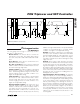
SCL
NOTE: TIMING IS REFERENCED TO V
IL(MAX)
AND V
IH(MIN)
.
SDA
STOP START REPEATED
START
t
BUF
t
HD:STA
t
HD:DAT
t
SU:DAT
t
SU:STO
t
HD:STA
t
SP
t
SU:STA
t
HIGH
t
R
t
F
t
LOW
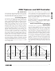
Figure 15. I
2
C Timing Diagram
I
2
C Communication
I
2
C Definitions
The following terminology is commonly used to
describe I
2
C data transfers.
Master Device: The master device controls the
slave devices on the bus. The master device gener-
ates SCL clock pulses and START and STOP condi-
tions.
Slave Devices: Slave devices send and receive
data at the master’s request.
Bus Idle or Not Busy: Time between STOP and
START conditions when both SDA and SCL are inac-
tive and in their logic-high states.
START Condition: A START condition is generated
by the master to initiate a new data transfer with a
slave. Transitioning SDA from high to low while SCL
remains high generates a START condition. See
Figure 15 for applicable timing.
STOP Condition: A STOP condition is generated by
the master to end a data transfer with a slave.
Transitioning SDA from low to high while SCL
remains high generates a STOP condition. See
Figure 15 for applicable timing.
Repeated START Condition: The master can use a
repeated START condition at the end of one data
transfer to indicate that it will immediately initiate a
new data transfer following the current one.
Repeated START conditions are commonly used
during read operations to identify a specific memory
address to begin a data transfer. A repeated START
condition is issued identically to a normal START
condition. See Figure 15 for applicable timing.
Bit Write: Transitions of SDA must occur during the
low state of SCL. The data on SDA must remain valid
and unchanged during the entire high pulse of SCL
plus the setup and hold-time requirements (Figure
15). Data is shifted into the device during the rising
edge of the SCL.
Bit Read: At the end of a write operation, the master
must release the SDA bus line for the proper amount
of setup time before the next rising edge of SCL dur-
ing a bit read (Figure 15). The device shifts out each
bit of data on SDA at the falling edge of the previous
SCL pulse and the data bit is valid at the rising edge
of the current SCL pulse. Remember that the master
generates all SCL clock pulses including when it is
reading bits from the slave.
Acknowledgement (ACK and NACK): An acknowl-
edge-ment (ACK) or not acknowledge (NACK) is
always the 9th bit transmitted during a byte transfer.
The device receiving data (the master during a read
or the slave during a write operation) performs an
ACK by transmitting a zero during the 9th bit. A
device performs a NACK by transmitting a one dur-
ing the 9th bit. Timing for the ACK and NACK is
identical to all other bit writes (Figure 15). An ACK is
the acknowledgment that the device is properly
receiving data. A NACK is used to terminate a read
sequence or as an indication that the device is not
receiving data.
PON Triplexer and SFP Controller
______________________________________________________________________________________ 29