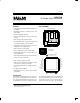
DS2153Q DS2153Q E1 Single–Chip Transceiver FEATURES PIN ASSIGNMENT • Complete E1(CEPT) PCM–30/ISDN–PRI transceiver FUNCTIONAL BLOCKS LONG & SHORT HAUL LINE INTERFACE line interface for clock/data recovery and waveshaping • 32–bit or 128–bit jitter attenuator • Generates line build–outs for both 120 ohm and 75 ohm lines • Frames to FAS, CAS, and CRC4 formats • Dual onboard two–frame elastic store slip buffers that ELASTIC STORES • Onboard FRAMER functionality PARALLEL CONTROL PORT can connect
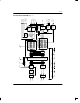
DS2153Q attenuator (selectable to either 32 bits or 128 bits) can be placed in either the transmit or receive data paths. The framer locates the frame and multiframe boundaries and monitors the data stream for alarms. It is also used for extracting and inserting signaling data, Si, and Sa–bit information. The device contains a set of 71 8–bit internal registers which the user can access and control the operation of the unit.
CS Jitter Attenuation Mux (can be placed in either the transmit or receive paths) Local Loopback ALE(AS) Remote Loopback AD0 – AD7 Framer Loopback RD(DS) INT1/INT2 HDB3 Encode AIS Generation WR(R/W) BPV Counter HDB3 Decoder Parallel Control Port (routed to all blocks) Synchronizer Transmit Side Formatter Alarm Detection Wave Shaping Clock/ Data Recovery Receive Side Framer E Bit Count CRC4 Error Count BTS Peak Detect 32.
DS2153Q PIN DESCRIPTION Table 1–1 PIN SYMBOL TYPE 1 2 3 4 AD4 AD5 AD6 AD7 I/O 5 RD(DS) I Read Input (Data Strobe). 6 CS I Chip Select. Must be low to read or write the port. 7 ALE(AS) I Address Latch Enable (Address Strobe). A positive going edge serves to demultiplex the bus. 8 WR(R/W) I Write Input (Read/Write). 9 RLINK O Receive Link Data. Outputs the full receive data stream including the Sa bits. See Section 13 for timing details. 10 RLCLK O Receive Link Clock.
DS2153Q PIN SYMBOL TYPE DESCRIPTION 20 BTS I Bus Type Select. Strap high to select Motorola bus timing; strap low to select Intel bus timing. This pin controls the function of the RD(DS), ALE(AS), and WR(R/W) pins. If BTS=1, then these pins assume the function listed in parenthesis (). 21 22 RTIP RRING – Receive Tip and Ring. Analog inputs for clock recovery circuitry; connects to a 1:1 transformer (see Section 12 for details). 23 RVDD – Receive Analog Positive Supply. 5.0 volts.
DS2153Q PIN SYMBOL TYPE DESCRIPTION 40 TCHCLK O Transmit Channel Clock. 256 KHz clock which pulses high during the LSB of each channel. Useful for parallel to serial conversion of channel data. See Section 13 for timing details. 41 42 43 44 AD0 AD1 AD2 AD3 I/O Address/Data Bus. A 8–bit multiplexed address/data bus.
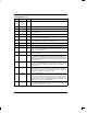
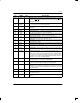
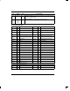
DS2153Q ADDRESS R/W 30 R 31 32 REGISTER NAME ADDRESS R/W REGISTER NAME Receive Signaling 1 40 R/W Transmit Signaling 1 R Receive Signaling 2 41 R/W Transmit Signaling 2 R Receive Signaling 3 42 R/W Transmit Signaling 3 33 R Receive Signaling 4 43 R/W Transmit Signaling 4 34 R Receive Signaling 5 44 R/W Transmit Signaling 5 35 R Receive Signaling 6 45 R/W Transmit Signaling 6 36 R Receive Signaling 7 46 R/W Transmit Signaling 7 37 R Receive Signaling 8 47 R
DS2153Q RCR1: RECEIVE CONTROL REGISTER 1 (Address=10 Hex) (MSB) RSMF (LSB) RSM RSIO – – FRC SYNCE RESYNC SYMBOL POSITION NAME AND DESCRIPTION RSMF RCR1.7 RSYNC Multiframe Function. Only used if the RSYNC pin is programmed in the multiframe mode (RCR1.6=1). 0=RSYNC outputs CAS multiframe boundaries 1=RSYNC outputs CRC4 multiframe boundaries RSM RCR1.6 RSYNC Mode Select. 0=frame mode (see the timing in Section 13) 1=multiframe mode (see the timing in Section 13) RSIO RCR1.
DS2153Q RCR2: RECEIVE CONTROL REGISTER 2 (Address=11 Hex) (MSB) Sa8S (LSB) Sa7S Sa6S Sa5S Sa4S RSCLKM RESE – SYMBOL POSITION NAME AND DESCRIPTION Sa8S RCR2.7 Sa8 Bit Select. Set to one to report the Sa8 bit at the RLINK pin; set to zero to not report the Sa8 bit. Sa7S RCR2.6 Sa7 Bit Select. Set to one to report the Sa7 bit at the RLINK pin; set to zero to not report the Sa7 bit. Sa6S RCR2.5 Sa6 Bit Select.
DS2153Q TSA1 TCR1.2 Transmit Signaling All Ones. 0=normal operation 1=force timeslot 16 in every frame to all ones TSM TCR1.1 TSYNC Mode Select. 0=frame mode (see the timing in Section 13) 1=CAS and CRC4 multiframe mode (see the timing in Section 13) TSIO TCR1.0 TSYNC I/O Select. 0=TSYNC is an input 1=TSYNC is an output Note: See Figure 13–9 for more details about how the Transmit Control Registers affect the operation of the DS2153Q.
DS2153Q THDB3 CCR1.6 Transmit HDB3 Enable. 0=HDB3 disabled 1=HDB3 enabled TG802 CCR1.5 Transmit G.802 Enable. See Section 13 for details. 0=do not force TCHBLK high during bit 1 of timeslot 26 1=force TCHBLK high during bit 1 of timeslot 26 TCRC4 CCR1.4 Transmit CRC4 Enable. 0=CRC4 disabled 1=CRC4 enabled RSM CCR1.3 Receive Signaling Mode Select. 0=CAS signaling mode 1=CCS signaling mode RHDB3 CCR1.2 Receive HDB3 Enable. 0=HDB3 disabled 1=HDB3 enabled RG802 CCR1.1 Receive G.802 Enable.
DS2153Q RSERC CCR2.3 RSER Control. 0=allow RSER to output data as received under all conditions 1=force RSER to one under loss of frame alignment conditions LOTCMC CCR2.2 Loss of Transmit Clock Mux Control. Determines whether the transmit side formatter should switch to the ever present RCLK if the TCLK should fail to transition (see Figure 1.1). 0=do not switch to RCLK if TCLK stops 1=switch to RCLK if TCLK stops RLB CCR2.1 Remote Loopback. 0=loopback disabled 1=loopback enabled LLB CCR2.
DS2153Q applied and is stable. Must be set and cleared again for a subsequent reset. Do not leave this bit set high. LIRST CCR3.3 Line Interface Reset. Setting this bit from a zero to a one will initiate an internal reset that affects the slicer, AGC, clock recovery state machine, and jitter attenuator. Normally this bit is only toggled on power–up. Must be cleared and set again for a subsequent reset. – CCR3.2 Not Assigned. Should be set to zero when written. TSCLKM CCR3.
DS2153Q RIR: RECEIVE INFORMATION REGISTER (Address=08 Hex) (MSB) TESF (LSB) TESE JALT RESF RESE CRCRC FASRC CASRC SYMBOL POSITION NAME AND DESCRIPTION TESF RIR.7 Transmit Elastic Store Full. Set when the elastic store fills and a frame is deleted. TESE RIR.6 Transmit Elastic Store Empty. Set when the elastic store empties and a frame is repeated. JALT RIR.5 Jitter Attenuator Limit Trip.
DS2153Q CRC4 SYNC COUNTER The CRC4 Sync Counter increments each time the 8 ms CRC4 multiframe search times out. The counter is cleared when the DS2153Q has successfully obtained synchronization at the CRC4 level. The counter can also be cleared by disabling the CRC4 mode (CCR1.0=0). This counter is useful for determining the amount of time the DS2153Q has been searching for synchronization at the CRC4 level. Annex B of CCITT G.
DS2153Q ALARM CRITERIA Table 4–1 ALARM SET CRITERIA CLEAR CRITERIA CCITT SPEC. RSA1 (receive signaling all ones) over 16 consecutive frames (one full MF) timeslot 16 contains less than 3 zeros over 16 consecutive frames (one full MF) timeslot 16 contains 3 or more zeros G.732 4.2 RSA0 (receive signaling all zeros) over 16 consecutive frames (one full MF) timeslot 16 contains all zeros over 16 consecutive frames (one full MF) timeslot 16 contains at least a single one G.732 5.
DS2153Q IMR1: INTERRUPT MASK REGISTER 1 (Address=16 Hex) (MSB) RSA1 (LSB) RDMA RSA0 RSLIP RUA1 RRA SYMBOL POSITION RSA1 IMR1.7 Receive Signaling All Ones. 0=interrupt masked 1=interrupt enabled RDMA IMR1.6 Receive Distant MF Alarm. 0=interrupt masked 1=interrupt enabled RSA0 IMR1.5 Receive Signaling All Zeros. 0=interrupt masked 1=interrupt enabled RSLIP IMR1.4 Receive Elastic Store Slip Occurrence. 0=interrupt masked 1=interrupt enabled RUA1 IMR1.3 Receive Unframed All Ones.
DS2153Q IMR2: INTERRUPT MASK REGISTER 2 (Address=17 Hex) (MSB) RMF (LSB) RAF TMF SEC TAF LOTC SYMBOL POSITION RMF IMR2.7 Receive CAS Multiframe. 0=interrupt masked 1=interrupt enabled RAF IMR2.6 Receive Align Frame. 0=interrupt masked 1=interrupt enabled TMF IMR2.5 Transmit Multiframe. 0=interrupt masked 1=interrupt enabled SEC IMR2.4 One Second Timer. 0=interrupt masked 1=interrupt enabled TAF IMR2.3 Transmit Align Frame. 0=interrupt masked 1=interrupt enabled LOTC IMR2.
DS2153Q VCR1: UPPER BIPOLAR VIOLATION COUNT REGISTER 1 (Address=00 Hex) VCR2: LOWER BIPOLAR VIOLATION COUNT REGISTER 2 (Address=01 Hex) (MSB) (LSB) V15 V14 V13 V12 V11 V10 V9 V8 VCR1 V7 V6 V5 V4 V3 V2 V1 V0 VCR2 SYMBOL POSITION NAME AND DESCRIPTION V15 VCR1.7 MSB of the 16–bit bipolar or code violation count V0 VCR2.0 LSB of the 16–bit bipolar or code violation count 5.
DS2153Q EBCR1: E–BIT COUNT REGISTER 1 (Address=04 Hex) EBCR2: E–BIT COUNT REGISTER 2 (Address=05 Hex) (MSB) (LSB) (note 1) (note 1) (note 1) (note 1) (note 1) (note 1) EB9 EB8 EBCR1 EB7 EB6 EB5 EB4 EB3 EB2 EB1 EB0 EBCR2 SYMBOL POSITION NAME AND DESCRIPTION EB9 EBCR1.1 MSB of the 10–bit E–Bit count EB0 EBCR2.0 LSB of the 10–bit E–Bit count NOTES: 1. The upper six bits of EBCR1 at address 04 are the least significant bits of the 12–bit FAS error counter. 5.
DS2153Q additional bits from the TLINK pin. If the user wishes to pass the Sa bits through the DS2153Q without them being altered, then the device should be set up to source all five Sa bits via the TLINK pin and the TLINK pin should be tied to the TSER pin. Please see the timing diagrams and the transmit data flow diagram in Section 13 for examples. receive stream and inserted into the transmit stream by the DS2153Q. Each of the 30 channels has four signaling bits (A/B/C/D) associated with it.
DS2153Q conditions. Their validity should be qualified by checking for synchronization at the CAS level. In CCS signaling mode, RS1 to RS16 can also be used to extract signaling information. Via the SR2.7 bit, the user will be informed when the signaling registers have been loaded with data. The user has 2 ms to retrieve the data before it is lost.
DS2153Q will be informed when the signaling registers need to be loaded with data. The user has 2 ms to load the data before the old data will be retransmitted. Via the CCR3.6 bit, the user has the option to use the Transmit Channel Blocking Registers (TCBRs) to determine on a channel by channel basis, which signaling bits are to be inserted via the TSRs (the corresponding bit in the TCBRs=1) and which are to be sourced from the TSER pin (the corresponding bit in the TCBRs=0).
DS2153Q 9.0 CLOCK BLOCKING REGISTERS The Receive Channel Blocking Registers (RCBR1/RCBR2/RCBR3/RCBR4) and the Transmit Channel Blocking Registers (TCBR1/TCBR2/TCBR3/ TCBR4) control the RCHBLK and TCHBLK pins respectively. The RCHBLK and TCHCLK pins are user programmable outputs that can be forced either high or low during individual channels. These outputs can be used to block clocks to a USART or LAPD controller in ISDN–PRI applications.
DS2153Q TCBR1/TCBR2/TCBR3/TCBR4: DEFINITION WHEN CCR3.6 = 1 (MSB) (LSB) CH20 CH4 CH19 CH3 CH18 CH2 CH17* CH1* TCBR1 CH24 CH8 CH23 CH7 CH22 CH6 CH21 CH5 TCBR2 CH28 CH12 CH27 CH11 CH26 CH10 CH25 CH9 TCBR3 CH32 CH16 CH31 CH15 CH30 CH14 CH29 CH13 TCBR4 * = CH1 and CH17 should be set to one to allow the internal TS1 register to create the CAS Multiframe Alignment Word and Spare/Remote Alarm bits. 10.
DS2153Q RAF: RECEIVE ALIGN FRAME REGISTER (Address=2F Hex) (MSB) (LSB) Si 0 0 1 1 SYMBOL POSITION Si RAF.7 International Bit. 0 RAF.6 Frame Alignment Signal Bit. 0 RAF.5 Frame Alignment Signal Bit. 1 RAF.4 Frame Alignment Signal Bit. 1 RAF.3 Frame Alignment Signal Bit. 0 RAF.2 Frame Alignment Signal Bit. 1 RAF.1 Frame Alignment Signal Bit. 1 RAF.0 Frame Alignment Signal Bit.
DS2153Q 1 TAF.3 Frame Alignment Signal Bit. 0 TAF.2 Frame Alignment Signal Bit. 1 TAF.1 Frame Alignment Signal Bit. 1 TAF.0 Frame Alignment Signal Bit. TNAF: TRANSMIT NON–ALIGN FRAME REGISTER (Address=21 Hex) (MSB) (LSB) Si 1 SYMBOL POSITION Si TNAF.7 International Bit. 1 TNAF.6 Frame Non–Alignment Signal Bit. A TNAF.5 Remote Alarm. Sa4 TNAF.4 Additional Bit 4. Sa5 TNAF.3 Additional Bit 5. Sa6 TNAF.2 Additional Bit 6. Sa7 TNAF.1 Additional Bit 7. Sa8 TNAF.
DS2153Q DJA LICR.1 Disable Jitter Attenuator. 0=jitter attenuator enabled 1=jitter attenuator disabled TPD LICR.0 Transmit Power Down. 0=normal transmitter operation 1=powers down the transmitter and 3–states the TTIP and TRING pins 12.1 Receive Clock and Data Recovery The DS2153Q contains a digital clock recovery system. See the DS2153Q Block Diagram in Section 1 and Figure 12.1 for more details. The DS2153Q couples to the receive E1 shielded twisted pair or COAX via a 1:1 transformer. See Table 12.
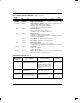
DS2153Q LINE BUILD OUT SELECT IN LICR Table 12–2 L2 L1 L0 0 0 0 0 0 0 APPLICATION TRANSFORMER RETURN LOSS Rt 75 ohm normal 1:1.15 step–up NM 0 ohms 1 120 ohm normal 1:1.15 step–up NM 0 ohms 1 0 75 ohm normal with protection resistors 1:1.15 step–up NM 8.2 ohms 0 1 1 120 ohm normal with protection resistors 1:1.15 step–up NM 8.2 ohms 1 0 0 75 ohm with high return loss 1:1.15 step–up 21 dB 27 ohms 1 1 0 75 ohm with high return loss 1:1.
DS2153Q DS2153Q will divide the attached crystal by either 3.5 or 4.5 instead of the normal 4 to keep the buffer from overflowing. When the device divides by either 3.5 or 4.5, it also sets the Jitter Attenuator Limit Trip (JALT) bit in the Receive Information Register (RIR.5). CRYSTAL SELECTION GUIDELINES Table 12–4 PARAMETER SPECIFICATION Parallel Resonant Frequency 8.192 MHz Mode Fundamental Load Capacitance 18 pF to 20 pF (18.
DS2153Q DS2153Q JITTER TOLERANCE Figure 12–2 1K UNIT INTERVALS (Ulpp) DS2153Q TOLERANCE 100 40 10 1.5 1 MINIMUM TOLERANCE LEVEL AS PER ITU G.823 0.2 0.1 1 10 20 100 1K 2.4K 10K 18K 100K FREQUENCY (Hz) DS2153Q TRANSMIT WAVEFORM TEMPLATE Figure 12–3 1.2 1.1 269 ns SCALED AMPLITUDE (in 75 ohm systems, 1.0 on the scale=2.37Vpeak in 120 ohm systems, 1.0 on the scale=3.00Vpeak) 1.0 0.9 0.8 0.7 G.703 TEMPLATE 194 ns 0.6 0.5 219 ns 0.4 0.3 0.2 0.1 0 –0.1 –0.
DS2153Q DS2153Q JITTER ATTENUATION Figure 12–4 0 dB JITTER ATTENUATION (dB) ITU G.7XX PROHIBITED AREA –20 dB –40 dB –60 dB 1 10 100 1K 10K 100K FREQUENCY (Hz) 13.0 TIMING DIAGRAMS/SYNCHRONIZATION FLOWCHART/TRANSMIT DATA FLOW DIAGRAM RECEIVE SIDE TIMING Figure 13–1 FRAME# 14 15 16 1 2 3 4 5 6 7 8 9 10 11 12 13 14 15 16 1 RSYNC1 RSYNC2 RLCLK3 RLINK4 NOTES: 1. RSYNC in the frame mode (RCR1.6=0). 2. RSYNC in the multiframe mode (RCR1.6=1). 3.
DS2153Q RECEIVE SIDE BOUNDARY TIMING (WITH ELASTIC STORES DISABLED) Figure 13–2 RCLK CHANNEL 32 RSER MSB CHANNEL 1 LSB Si 1 A Sa4 Sa5 Sa6 Sa7 Sa8 MSB Sa4 Sa5 Sa6 Sa7 Sa8 CHANNEL 2 RSYNC RCHCLK RCHBLK1 RLINK RLCLK2 RLCLK3 RLCLK4 NOTES: 1. RCHBLK is programmed to block channel 2. 2. RLINK is programmed to output the Sa4 bits. 3. RLINK is programmed to output the SA4 and SA8 bits. 4. RLINK is programmed to output the Sa5 and Sa7 bits. 5. Shown is a non–align frame boundary.
DS2153Q 1.544 MHz BOUNDARY TIMING WITH ELASTIC STORE(S) ENABLED Figure 13–3 SYSCLK RSER1, TSER CHANNEL 23/31 CHANNEL 24/32 LSB MSB CHANNEL 1/2 LSB F MSB RSYNC2 RSYNC3 RCHCLK RCHBLK4 NOTES: 1. Data from the E1 channels 1, 5, 9, 13, 17, 21, 25, and 29 is dropped (channel 2 from the E1 link is mapped to channel 1 of the T1 link, etc.) and the F–bit position is added (forced to one). 2. RSYNC is in the output mode (RCR1.5=0). 3. RSYNC is in the input mode (RCR1.5=1). 4.
DS2153Q TRANSMIT SIDE TIMING Figure 13–5 FRAME# 14 15 16 1 2 3 4 5 6 7 8 9 10 11 12 13 14 15 16 1 2 3 4 5 6 TSYNC1 TSYNC2 TCLK3 TLINK3 NOTES: 1. TSYNC in the frame mode (TCR1.1=0). 2. TSYNC in the multiframe mode (TCR1.1=1). 3. TLINK is programmed to source only the Sa4 bit. 4. This diagram assumbes both the CAS MF and the CRC4 begin with the align frame.
DS2153Q TRANSMIT SIDE BOUNDARY TIMING Figure 13–6 TCLK CHANNEL 1 TSER LSB Si 1 A CHANNEL 2 Sa4 Sa5 Sa6 Sa7 Sa8 MSB LSB MSB TSYNC1 TSYNC2 TCHCLK TCHBLK3 TLCLK4 TLINK4 Don’t Care Don’t Care TLCLK5 TLINK5 Don’t Care Don’t Care NOTES: 1. TSYNC is in the input mode (TCR1.0=0). 2. TSYNC is in the output mode (TCR1.0=1). 3. TCHBLK is programmed to block channel 2. 4. TLINK is programmed to source the Sa4 bits. 5. TLINK is programmed to source the Sa7 and Sa8 bits. 6.
DS2153Q G.802 TIMING Figure 13–7 TIMESLOT# 30 31 0 1 2 3 4 5 6 7 8 9 10 11 12 13 14 15 16 17 18 19 20 21 22 23 24 25 26 27 28 29 30 31 0 1 2 3 4 RSYNC/ TSYNC RCHCLK/ TCHCLK RCHBLK/ TCHBLK1 DETAIL RCLK/TCLK TIMESLOT 25 RSER/TSER TIMESLOT 26 LSB MSB RCHCLK/TCHCLK RCHBLK/TCHCLK NOTE: 1. RCHBLK or TCHBLK is programmed to pulse high during timeslots 1 to 15, 17 to 25, and during bit 1 of timeslot 26.
DS2153Q DS2153Q SYNCHRONIZATION FLOWCHART Figure 13–8 POWER UP RLOS=1 RLOS=1 FAS SYNC CRITERIA MET FASSA=0 RESYNC IF RCR1.1=0 CAS MULTIFRAME SEARCH (IF ENABLED INCREMENT CRC4 SYNC COUNTER; CRC4SA=0 8 MS TIME OUT CRC4 MULTIFRAME SEARCH (IF ENABLED VIA CCR.0) CRC4SA=1 CRC4 SYNC CRITERIA MET; CRC4SA=0; RESET CRC4 SYNC COUNTER SET FASRC (RIR.1) 022697 38/48 FAS RESYNC CRITERIA MET CHECK FOR FAS FRAMING ERROR (DEPENDS ON RCR1.2) CRC4 RESYNC CRITERIA MET (RIR.
DS2153Q DS2153Q TRANSMIT DATA FLOW Figure 13–9 TSER RSER (note 1) TLINK TAF TNAF 0 1 TIMESLOT 0 PASS–THROUGH (TCR1.6) 0 1 Si BIT INSERTION CONTROL (TCR1.3) RECEIVE SIDE CRC4 ERROR DETECTOR CRC4 MULTIFRAME ALIGNMENT WORD GENERATION (CCR1.4) 1 0 TIDR E–BIT GENERATION (TCR2.1) 0 0 1 1 TIR FUNCTION SELECT (CCR3.5) Sa BIT INSERTION CONTROL (TCR2.3 THRU TCR2.7) AUTO REMOTE ALARM GENERATION (CCR2.
DS2153Q ABSOLUTE MAXIMUM RATINGS* Voltage on Any Pin Relative to Ground Operating Temperature Storage Temperature Soldering Temperature –1.0V to +7.0V 0°C to 70°C (–40°C to +85°C for DS2153QN) –55°C to +125°C 260°C for 10 seconds * This is a stress rating only and functional operation of the device at these or any other conditions above those indicated in the operation sections of this specification is not implied.
DS2153Q AC CHARACTERISTICS – PARALLEL PORT PARAMETER (0°C to 70°C; VDD=5V + 5%) (–40°C to +85°C; VDD=5V +5%/–4% for DS2153QN) SYMBOL MIN tCYC 250 ns Pulse Width, DS Low or RD High PWEL 150 ns Pulse Width, DS High or RD Low PWEH 100 ns Cycle Time TYP MAX Input Rise/Fall Times tR, tF R/W Hold Time tRWH 10 ns R/W Setup Time Before DS High tRWS 50 ns CS Setup Time Before DS, WR or RD active tCS 20 ns CS Hold Time tCH 0 ns Read Data Hold Time tDHR 10 Write Data Hold Time
DS2153Q INTEL READ BUS AC TIMING Figure 14–1 tCYC PWASH ALE tASD WR tASD tASED PWEH PWEL RD tCS tCH CS tDDR tASL tDHR AD0-AD7 tAHL INTEL WRITE BUS AC TIMING Figure 14–2 tCYC PWASH ALE tASD RD WR tASD tASED PWEH PWEL tCH tCS CS tASL tDHW AD0-AD7 tAHL 022697 42/48 tDSW
DS2153Q MOTOROLA BUS AC TIMING Figure 14–3 PWASH AS PWEH DS tASD tASED PWEL tCYC tRWS tRWH R/W tASL tDDR tDHR AD0-AD7 (READ) tAHL AD0-AD7 (WRITE) tCH tCS CS tASL tDSW tAHL tDHW 022697 43/48
DS2153Q AC CHARACTERISTICS – RECEIVE SIDE PARAMETER SYMBOL (0°C to 70°C; VDD=5V ± 5%) (–40°C to +85°C; VDD=5V +5%/–4% for DS2153QN) MIN TYP MAX UNITS ALCKI/RCLK Period tCP RCLK Pulse Width tCH tCL RCLK Pulse Width tCH tCL SYSCLK Period tSP tSP SYSCLK Pulse Width tSH tSL 50 50 RSYNC Set Up to SYSCLK Falling tSU 25 RSYNC Pulse Width tPW 50 SYSCLK Rise/Fall Times tR, tF 25 ns Delay RCLK or SYSCLK to RSER Valid tDD 70 ns Delay RCLK or SYSCLK to RCHCLK tD1 50 ns Delay RCLK or
DS2153Q RECEIVE SIDE AC TIMING Figure 14–4 tCP tCL tCH tSL tSH RCLK tR tF SYSCLK tSP tDD MSB OF CHANNEL 1 RSER tD1 RCHCLK tD2 RCHBLK tD3 RSYNC1 tPW tSU RSYNC2 tD4 RLCLK3 tD5 RLINK3 NOTES: 1. RSYNC is in the output mode (RCR1.5=0). 2. RSYNC is in the input mode (RCR1.5=1). 3. RLCLK and RLINK only have a timing relationship to RCLK; no timing relationship between RLCLK/RLINK and RSYNC is implied. 4.
DS2153Q AC CHARACTERISTICS – TRANSMIT SIDE PARAMETER SYMBOL TCLK Period tP (0°C to 70°C; VDD=5V + 5%) (–40°C to +85°C; VDD=5V +5%/–4% for DS2153QN) MIN TYP MAX 488 UNITS NOTES ns TCLK Pulse Width tCH tCL 75 75 ns ns TSER, TLINK Set Up to TCLK Falling tSU 25 ns 1 TSER, TLINK Hold from TCLK Falling tHD 25 ns 1 TSYNC Setup to TCLK Falling tHD 25 TSYNC Pulse Width tPW 25 TCLK Rise/Fall Times tR, tF 25 ns Delay TCLK to TCHCLK tD1 50 ns Delay TCLK to TCHBLK tD2 50 ns De
DS2153Q TRANSMIT SIDE AC TIMING Figure 14–5 tP tCL tF tR tCH TCLK TSER4 LSB MSB tHD tD1 tSU TCHCLK tD2 TCHBLK tD3 TSYNC1 tPW tSU TSYNC2 tD4 TLCLK3 tHD tSU TLINK3 NOTES: 1. TSYNC is in the output mode (TCR1.0=1). 2. TSYNC is in the input mode (TCR1.0=0). 3. No timing relationship between TSYNC and TLCLK/TLINK is implied. 4. TSER is sampled on the falling edge of SYSCLK if the transmit side elastic store is enabled.
DS2153Q DS2153Q E1 SINGLE–CHIP TRANSCEIVER 44–PIN PLCC E E1 B N 1 .075 MAX D1 D D2 NOTE 1 B1 CH1 .150 MAX e1 C E2 A2 NOTE1: PIN 1 IDENTIFIER TO BE LOCATED IN ZONE INDICATED. INCHES DIM MIN MAX A 0.165 0.180 A1 0.090 0.120 A2 0.020 – B 0.026 0.033 B1 0.013 0.021 C 0.009 0.012 CH1 0.042 0.048 D 0.685 0.695 D1 0.650 0.656 D2 0.590 0.630 E 0.685 0.695 E1 0.650 0.656 E2 0.590 0.630 e1 N 022697 48/48 0.