
Instruction Manual


DS2406
18 of 31
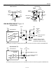
DS2406 EQUIVALENT CIRCUIT Figure 11
1-Wire Interface
PIO
Ground
PIO Channel
Reset
D
"1"
Q
Q
Activity
Latch
DQ
Q
1-Wire DATA
Channel
Flip-Flop
to PIO-
Control
10 M
W
Typ.
from PIO-
Control
R
Edge
Detector
DATA
RX
TX
100
W
MOSFET
Ground
5 µA
Typ.
BUS MASTER CIRCUIT Figure 12
A) Open Drain
12V
Open Drain
Port Pin
S
D
D
S
470 pF
D
S
PGM
DS
2N7000
2N7000
2N7000
VP0300L
OR
VP0106N3
OR
BSS110
Capacitor added to reduce
coupling on data line due to
programming signal switching
V
PUP
RX
TX
B) Standard TTL
TTL-Equivalent
Port Pins
5 k
W
12V
(10 mA min.)
to data connection
of DS2406
PROGRAMMING PULSE
The diode and programming circuit are not required if one does not intend to program the EPROM cell
s
V
PUP
RX
TX
DD
V
5 k
W
to data connection
of DS2406
DD
V
DS5000 OR 8051-
EQUIVALENT
5 k
W
10 k W
10 k W
BUS MASTER
BUS MASTER
The interface is reduced to the pull-up resistor if one does not intend to program the EPROM cells.5k
W