
Owner's manual
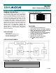


DS2705: SHA-1 Authentication Master
5 of 18
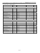
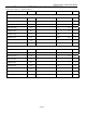
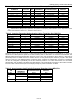
AC ELECTRICAL CHARACTERISTICS
(2.5V £ V
DD
£ 5.5V, T
A
= -20°C to +85°C.)
PARAMETER SYMBOL CONDITIONS MIN TYP MAX UNITS
Programming Pulse Width t
PPW
17 ms
Programming Pulse Rise Time t
PPR
(Note 8) 0.5 5
ms
Programming Pulse Fall Time t
PPF
(Note 8) 0.5 5
ms
Strong Pullup Delay Time t
SPUD
2 10
ms
Strong Pullup Period t
SPUP
24 34 48 ms
Challenge Delay Time t
CHD
45 65 85 ms
Authentication Attempt Time t
AAT
(Note 9) 61 490 ms
FAIL Pin Pulse Frequency
t
FPF
FOM = 1, 50% duty cycle 1.5 2 2.5 Hz
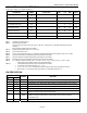
Note 1:
All voltages are referenced to V
SS
.
Note 2:
IDD3 Sleep mode conditions:
CHAL pin inactive OR (CHAL active AND (PAA = 0 AND PPT = 00 AND FOM = 0 AND Initial Authentication sequence
complete))
[Above conditions disable the internal oscillator]
Note 3:
Programming temperature range is T
A
= 0°C to 50°C.
Note 4:
5 years data retention at 70°C
Note 5:
If CHAL pin left unconnected, CHP bit = 0 required for an authentication attempt to be initiated on power up. See Table 1.
Note 6:
Typical Communication mode MDQ pullup behavior equivalent to 3kW resistor.
Note 7:
Typical Computation mode MDQ pullup behavior approximates a 50W resistor.
Note 8:
Exceeding maximum rise and fall time specifications may affect device reliability.
Note 9:
t
AAT
= Retries per Attempt x (264bits x 90ms + 3 x (t
MRSTL
+ t
RSTH
) + t
SPUD
) = [1 to 8] x (23.7ms + 3.54ms + 34ms)
MAX[7 retries]: 490ms, MIN[no retries]: 61ms with standard timings
Note 10:
1. 1-Wire Master timings based on ±25% clock tolerance from nominal.
2. t
RPDT
[defined in design documentation] = t
MRSTL
+ t
MRSTH
3. t
MPDL-MAX
= t
MRSTH-MIN
– t
MPDH-MAX,
represents the maximum presence pulse low time allowed from the slave.
4. Bus rise time of ~1ms required to settle to logic high by t
MRDV
after MDQ released at t
MLOW1
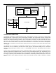
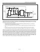
PIN DESCRIPTION
PIN
mMAX
TDFN
SYMBOL FUNCTION
1 1 CHAL Challenge Strobe Input Pin. Initiates authentication. Active level/edge set by CHP bit.
2 2
PASS
Authentication “PASS” Result Open-Drain Output Pin
3 3
FAIL
Authentication “FAIL” Result Open-Drain Output Pin (Programmable As Low Or Pulse)
4 4
V
SS
Supply Return Pin, GND Reference for Logic Signals
5 5
V
PP
EEPROM Programming Voltage Input
6 6 SDQ
Slave Serial interface Data I/O Pin. Bidirectional data transmit and receive at 16kbps or
143kbps. Bus master must provide a weak pullup.
7 7 MDQ
Master Serial interface Data I/O Pin. Bidirectional data transmit and receive at 16kbps or
143kbps. Provides a weak pullup in communication mode and strong pullup in
computation mode.
8 8
V
DD
Supply Input Pin. Bypass to V
SS
with 0.1mF capacitor.