
Manual


DS31256
169 of 181
AC CHARACTERISTICS: LAYER 1 PORTS
(V
DD
= 3.0V to 3.6V, T
A
= 0°C to +70°C.)
PARAMETER SYMBOL CONDITIONS MIN TYP MAX UNITS
(Note 9) 100
RC/TC Clock Period t1
(Note 10) 19
ns
(Note 9) 40
RC/TC Clock Low Time t2
(Note 10) 8
ns
(Note 9) 40
RC/TC Clock High Time t3
(Note 10) 8
ns
(Note 9) 5
RD Setup Time to the Falling Edge or
Rising Edge of RC
t4
(Note 10) 2
ns
RS/TS Setup Time from the Falling
Edge or Rising Edge of RC/TC
t4 (Note 9) 5 t1 - 10 ns
(Note 9) 5 RD Hold Time from the Falling Edge or
Rising Edge of RC
t5
(Note 10) 5
ns
RS/TS Hold Time from the Falling Edge
or Rising Edge of RC/TC
t5 (Note 9) 5 t1 - 10 ns
(Note 9) 5 25 Delay from the Rising Edge or Falling
Edge of TC to Data Valid on TD
t6
(Note 10) 3 15
ns
Note 9: Ports 0 to 15 in applications running up to 10MHz.
Note 10: Port 0, 1, or 2 running in applications up to 52MHz.
Note 11: Aggregate, maximum bandwidth and port speed for the DS31256 are directly proportional to PCLK frequency. Throughput
measurements are made at PCLK = 33MHz.
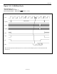
Figure 13-1. Layer 1 Port AC Timing Diagram
RC[n] / TC[n]
Normal Mode
RD[n] / RS[n] /
TS[n]
TD[n]
t4 t5
t6
t1
t2 t3
RC[n] / TC[n]
Inverted Mode
l1 ac
Note: TC and RC are independent of each other. In the above timing diagram, all the signals beginning with “T” reference the
transmit clock TC; all signals beginning with “R” reference the receive clock RC.