PRELIMINARY DS3134 Chateau – Channelized T1 And E1 And HDLC Controller www.dalsemi.
DS3134 There are 16 HDLC Engines (one for each port) that are capable of operating at speeds up to 8.192 Mbps in channelized mode and up to 10 Mbps in unchannelized mode. There are also two Fast HDLC Engines, which only reside on Ports 0 and 1 and they are capable of operating at speeds up to 52 Mbps.
DS3134 REVISION HISTORY Version 1 (1/30/98) Original release. Version 2 (4/4/98) 1. Assigned signals to leads (Section 2.1). 2. Added more information to Sections 1, 5, 7, and 10. 3. Removed the P3VEN signal pin (Section 2.1 and 2.5). 4. Added FIFO Priority Control bits to the MC register (Section 4.2). 5. Added Abort and Bit Stuffing Control bits to the RHCD and THCD registers (Section 6.2). 6. Changed the Absolute Maximum Voltage Rating and IOH numbers (Section 12). 7.
DS3134 Version 6 (05/01/00) Rev B1/B2 silicon release 1. Typo correction on the following pages: 7, 53, 61, 80, 107, 114 and 115 2. Add (notes) clarifications on the following pages: 60, 63, 73, 76, 87, 88, 90, 93, 95, 110, 111 and 117 3. Update Layer 1 configuration restrictions for silicon Rev B1/B2 release, on page 10. 4. Update reset wait cycles on page 11. 5. Remove bit 1 form register RDMAQ on page 97. 6. Local Bus timing update, corrected t3 and t6 on page 169. 7.
DS3134 TABLE OF CONTENTS Section 1: Introduction……………………………………………………………………………………..7 Section 2: Signal Description…………………………………………………………………………… 2.1 Overview / Signal Lead List………………………………………………………………… 2.2 Serial Port Interface Signal Description…………………………………………………… 2.3 Local Bus Signal Description………………………………………………………………. 2.4 JTAG Signal Description…………………………………………………………………… 2.5 PCI Bus Signal Description………………………………………………………………… 2.6 Supply & Test Signal Description…………………...……………………………………..
DS3134 Section 7: FIFO………………………………………………………………………………………… 85 7.1 General Description & Example…………………………………………………………. 85 7.2 FIFO Register Description……………………………………………………………….. 87 Section 8: DMA………………………………………………………………………………………… 96 8.0 Introduction………………………………………………………………………………… 96 8.1 Receive Side………………………………………………………………………………. 97 8.1.1 Overview………………………………………………………………………. 97 8.1.2 Packet Descriptors……………………………………………………………. 103 8.1.3 Free Queue……………………………………………………………………. 105 8.1.
DS3134 SECTION 1: INTRODUCTION The DS3134 Chateau device is a 256 channels HDLC controller. The primary features of the device are listed in Table 1A. This data sheet is split in Sections along the major the blocks of the device as shown in Figure 1A. Throughout the data sheet, certain terms will be used and these terms are defined in Table 1B. The DS3134 device is designed to meet certain specifications and a listing of these governing specifications is shown in Table 1C.
DS3134 DS3134 FEATURE LIST Table 1A Layer Can Support Up to 64 T1 or E1 Data Streams or Two T3 Data Streams One 16 Independent Physical Ports all Capable of Speeds Up to 10 MHz Two of These Ports are also Capable of Speeds Up to 52 MHz Each Port can be Independently Configured for Either Channelized or Unchannelized Operation Each Physical Channelized Port can Handle One, Two, or Four T1 or E1 Data Streams Supports N x 64 kbps and N x 56 kbps Onboard V.
DS3134 Local Can Operate as a Bridge from the PCI Bus or a Configuration Bus Bus In Bridge Mode; can arbitrate for the Bus 8 or 16 Bits Wide In Bridge Mode, Supports a 1M Byte Address Space Supports both Intel and Motorola Bus Timing JTAG TEST ACCESS 3.
DS3134 DATA SHEET DEFINITIONS Table 1B Acronym Or Term Definition BERT Descriptor Dword DMA FIFO HDLC Host n/a V.54 Bit Error Rate Tester. A message passed back and forth between the DMA and the Host. Double Word. A 32-bit data entity. Direct Memory Access. First In First Out. Temporary memory storage scheme. High level Data Link Control. The main controller that resides on the PCI Bus. Not Assigned. A pseudorandom pattern used to control loopbacks (see ANSI T1.
DS3134 In the receive path, the following process occurs. The HDLC Engines collect the incoming data into 32-bit dwords and then signal the FIFO that the engine has data to transfer to the FIFO. The 16 ports are priority decoded (Port 0 gets the highest priority) for the transfer of data from the HDLC Engines to the FIFO Block.
DS3134 When the DMA begins burst writing data into the FIFO, it will try to completely fill the FIFO with HDLC packet data even if it that means writing multiple packets. Once the FIFO detects that the DMA has filled it to beyond the Low Water Mark (or an EOF is reached), the FIFO will begin transferring 32-bit dwords to the HDLC Engine. One of the unique attributes of the DS3134 is the structure of the DMA.
DS3134 DS3134 RESTRICTIONS FOR REV B1/B2 SILICON Table 1D Port maximum of 16 channelized and unchannelized physical ports Unchannelized ports 0 & 1: maximum data rate of 52 Mbps port 2 to 15: maximum data rate of 10 Mbps Channelized Channelized and with frame interleave interfaces or a minimum of two/multiple of two consecutive DS0 time slot assigned to one HDLC channel: 40 T1/E1 channels Channelized Channelized and with byte interleave interfaces: 32 T1/E1 channels Throughput maximum receive: 104
DS3134 INITIALIZATION On a system reset (which can be invoked by either hardware action via the PRST* signal or software action via the RST control bit in the Master Reset and ID register), all of the internal device configuration register are set to zero (0000h). Please note that the Local Bus Bridge Mode Control register (LBBMC) is not affected by software invoked system reset, it will be forced to all zeros only by hardware reset.
DS3134 INDIRECT REGISTERS Table 1E Register Name (Acronym) Channelized Port registers (CP0RD to CP15RD) Number of Indirect Registers 6144 (16 Ports x 128 DS0 Channels x 3 Registers for each DS0 Channel) Receive HDLC Channel Definition register (RHCD) 256 (one for each HDLC Channel) Transmit HDLC Channel Definition register (THCD) 256 (one for each HDLC Channel) Receive DMA Configuration register (RDMAC) 1536 (one for each HDLC Channel) Transmit DMA Configuration register (TDMAC) 3072 (one for each
DS3134 SECTION 2: SIGNAL DESCRIPTION 2.1 OVERVIEW / SIGNAL LEAD LIST This section describes the input and output signals on the DS3134. Signal names follow a convention that is shown in Table 2.1A. Table 2.1B lists all of the signals, their signal type, description, and lead location. Signal Naming Convention Table 2.1A First Letter R T L J P Signal Category Receive Serial Port Transmit Serial Port Local Bus JTAG Test Port PCI Bus Section 2.2 2.2 2.3 2.4 2.
DS3134 Lead K19 V20 U20 T18 T19 T20 R18 P17 R19 R20 P18 P19 P20 N18 N19 N20 M17 L18 L19 M18 K20 M19 H18 K18 H19 A2 A8 A11 A19 B2 B18 J18 J19 K1 K2 K3 L1 L2 L3 M20 U14 W2 W9 Y1 Y19 Symbol LCS* LD0 LD1 LD2 LD3 LD4 LD5 LD6 LD7 LD8 LD9 LD10 LD11 LD12 LD13 LD14 LD15 LHLDA(LBG*) LHOLD(LBR*) LIM LINT* LMS LRD*(LDS*) LRDY* LWR*(LR/W*) NC NC NC NC NC NC NC NC NC NC NC NC NC NC NC NC NC NC NC NC Type I I/O I/O I/O I/O I/O I/O I/O I/O I/O I/O I/O I/O I/O I/O I/O I/O I O I I/O I I/O I I/O - Signal Description Local
DS3134 Lead V17 U16 Y18 W17 V16 Y17 W16 V15 W15 V14 Y15 W14 Y14 V13 W13 Y13 V9 U9 Y8 W8 V8 Y7 W7 V7 U7 V6 Y5 W5 V5 Y4 Y3 U5 Y16 V12 Y9 W6 Y2 Symbol PAD0 PAD1 PAD2 PAD3 PAD4 PAD5 PAD6 PAD7 PAD8 PAD9 PAD10 PAD11 PAD12 PAD13 PAD14 PAD15 PAD16 PAD17 PAD18 PAD19 PAD20 PAD21 PAD22 PAD23 PAD24 PAD25 PAD26 PAD27 PAD28 PAD29 PAD30 PAD31 PCBE0* PCBE1* PCBE2* PCBE3* PCLK Type I/O I/O I/O I/O I/O I/O I/O I/O I/O I/O I/O I/O I/O I/O I/O I/O I/O I/O I/O I/O I/O I/O I/O I/O I/O I/O I/O I/O I/O I/O I/O I/O I/O I/O I/O I/
DS3134 Lead V11 V4 W3 Y12 W11 Y10 V18 Y20 W19 B1 D1 F2 H2 M1 P1 P4 V1 B17 B16 C14 D12 A10 B8 B6 C5 D2 E2 G3 J4 M3 R1 T2 U3 D16 C15 A14 B12 C10 A7 D7 A3 C2 E3 F1 H1 Symbol PPERR* PREQ* PRST* PSERR* PSTOP* PTRDY* PXAS* PXBLAST* PXDS* RC0 RC1 RC2 RC3 RC4 RC5 RC6 RC7 RC8 RC9 RC10 RC11 RC12 RC13 RC14 RC15 RD0 RD1 RD2 RD3 RD4 RD5 RD6 RD7 RD8 RD9 RD10 RD11 RD12 RD13 RD14 RD15 RS0 RS1 RS2 RS3 Type I/O O I O I/O I/O O O O I I I I I I I I I I I I I I I I I I I I I I I I I I I I I I I I I I I I Signal Description P
DS3134 Lead M2 P2 R3 T4 C17 A16 B14 C12 B10 C8 A5 B4 D3 E1 G2 J3 N1 P3 U1 V2 A18 D14 C13 A12 A9 B7 C6 D5 C1 G4 H3 J1 N3 T1 U2 V3 C16 A15 A13 C11 C9 C7 A4 B3 C3 Symbol RS4 RS5 RS6 RS7 RS8 RS9 RS10 RS11 RS12 RS13 RS14 RS15 TC0 TC1 TC2 TC3 TC4 TC5 TC6 TC7 TC8 TC9 TC10 TC11 TC12 TC13 TC14 TC15 TD0 TD1 TD2 TD3 TD4 TD5 TD6 TD7 TD8 TD9 TD10 TD11 TD12 TD13 TD14 TD15 TEST Type I I I I I I I I I I I I I I I I I I I I I I I I I I I I O O O O O O O O O O O O O O O O I Signal Description Receive Serial Sync for Port
DS3134 Lead E4 F3 G1 J2 N2 R2 T3 W1 A17 B15 B13 B11 B9 A6 B5 C4 D6 D10 D11 D15 F4 F17 K4 K17 L4 L17 R4 R17 U6 U10 U11 U15 A1 D4 D8 D9 D13 D17 H4 H17 J17 M4 N4 N17 U4 Symbol TS0 TS1 TS2 TS3 TS4 TS5 TS6 TS7 TS8 TS9 TS10 TS11 TS12 TS13 TS14 TS15 VDD VDD VDD VDD VDD VDD VDD VDD VDD VDD VDD VDD VDD VDD VDD VDD VSS VSS VSS VSS VSS VSS VSS VSS VSS VSS VSS VSS VSS Type I I I I I I I I I I I I I I I I - Signal Description Transmit Serial Sync for Port 0. Transmit Serial Sync for Port 1.
DS3134 Lead U8 U12 U13 U17 Symbol VSS VSS VSS VSS Type - Signal Description Ground Reference. Ground Reference. Ground Reference. Ground Reference. 2.2 SERIAL PORT INTERFACE SIGNAL DESCRIPTION Signal Name: RC0 / RC1 / RC2 / RC3 / RC4 / RC5 / RC6 / RC7 / RC8 / RC9 / RC10 / RC11 / RC12 / RC13 / RC14 / RC15 Signal Description: Receive Serial Clock Signal Type: Input Data can be clocked into the device either on falling edges (normal clock mode) or rising edges (inverted clock mode) of RC.
DS3134 RS SAMPLED EDGE Table 2.
DS3134 2.3 LOCAL BUS SIGNAL DESCRIPTION Signal Name: LMS Signal Description: Local Bus Mode Select Signal Type: Input This signal should be tied low when the device is to be operated either with no Local Bus access or if the Local Bus will be used to act as a bridge from the PCI bus. This signal should be tied high if the Local Bus is to be used by an external host to configure the device.
DS3134 Signal Name: LA0 to LA19 Signal Description: Local Bus Non-Multiplexed Address Bus Signal Type: Input / Output (tri-state capable) In the PCI Bridge Mode (LMS = 0), these signals are outputs that will be asserted on the rising edge of LCLK to indicate which address to be written to or read from. These signals will be tri-stated when the Local Bus is not currently involved in a bus transaction and driven when a bus transaction is active.
DS3134 Signal Name: LRDY* Signal Description: Local Bus PCI Bridge Ready [PCI Bridge Mode Only] Signal Type: Input This active low signal is sampled on the rising edge of LCLK to determine when a bus transaction is complete. This signal is only examined when a bus transaction is taking place. This signal is ignored when the Local Bus is in the Configuration Mode (LMS = 1) and should be tied high.
DS3134 Signal Name: LCLK Signal Description: Local Bus Clock [PCI Bridge Mode Only] Signal Type: Output (tri-state capable) This signal outputs a buffered version of the clock applied at the PCLK input. All Local Bus signals are generated and sampled from this clock. This output is tri-stated when the Local Bus is in the Configuration Mode (LMS = 1). It can be disabled in the PCI Bridge Mode via the Local Bus Bridge Mode Control Register (LBBMC).
DS3134 Signal Name: JTMS Signal Description: JTAG IEEE 1149.1 Test Mode Select Signal Type: Input (with internal 10k pull up) This signal is sampled on the rising edge of JTCLK and is used to place the test port into the various defined IEEE 1149.1 states. If not used, this signal should be pulled high. This signal has an internal pullup. 2.
DS3134 Signal Description: PCI Bus Parity Signal Type: Input / Output (tri-state capable) This signal provides information on even parity across both the PAD address/data bus and the PCBE bus command/byte enable bus. When the device is an initiator, this signal is an output for writes and input for reads and is updated on the rising edge of PCLK. When the device is a target, this signal is input for writes and an output for reads and is sampled on the rising edge of PCLK.
DS3134 Signal Name: PSTOP* Signal Description: PCI Stop Signal Type: Input / Output (tri-state capable) This active low signal is created by the target to signal to the initiator that it requests the initiator stop the current bus transaction. When the device is a target, this signal is an output and is updated on the rising edge of PCLK. When the device is an initiator, this signal is input and is sampled on the rising edge of PCLK.
DS3134 Signal Name: PSERR* Signal Description: PCI System Error Signal Type: Output (open drain) This active low signal reports any parity errors that occur during the address phase. PSERR* can be enabled and disabled via the PCI Configuration Registers. This signal is updated on the rising edge of PCLK.
DS3134 2.6 SUPPLY & TEST SIGNAL DESCRIPTION Signal Name: TEST Signal Description: Factory Test Input Signal Type: Input (with internal 10k pull up). This input should be left open circuited by the user. Signal Name: VDD Signal Description: Positive Supply Signal Type: n/a 3.3V (+/- 10%). All VDD signals should be tied together. Signal Name: VSS Signal Description: Ground Reference Signal Type: n/a All VSS signals should be tied to the local ground plane.
DS3134 SECTION 3: MEMORY MAP 3.0 INTRODUCTION All addresses within the memory map on dword boundaries even though all of the internal device configuration registers are only one word (16 bits) wide. The memory map consumes an address range of 4 kB (12 bits). When the PCI Bus is the Host (i.e.
DS3134 3.2 RECEIVE PORT REGISTERS (1XX) Offset/ Address 0100 0104 0108 010C 0110 0114 0118 011C 0120 0124 0128 012C 0130 0134 0138 013C Acronym Register Name Section RP0CR RP1CR RP2CR RP3CR RP4CR RP5CR RP6CR RP7CR RP8CR RP9CR RP10CR RP11CR RP12CR RP13CR RP14CR RP15CR Receive Port 0 Control Register. Receive Port 1 Control Register. Receive Port 2 Control Register. Receive Port 3 Control Register. Receive Port 4 Control Register. Receive Port 5 Control Register. Receive Port 6 Control Register.
DS3134 3.
DS3134 3.6 BERT REGISTERS (5XX) Offset/ Address 0500 0504 0508 050C 0510 0514 0518 051C Acronym Register Name Section BERTC0 BERTC1 BERTRP0 BERTRP1 BERTBC0 BERTBC1 BERTEC0 BERTEC1 BERT Control 0. BERT Control 1. BERT Repetitive Pattern Set 0 (lower word). BERT Repetitive Pattern Set 1 (upper word). BERT Bit Counter 0 (lower word). BERT Bit Counter 1 (upper word). BERT Error Counter 0 (lower word). BERT Error Counter 1 (upper word). 5.6 5.6 5.6 5.6 5.6 5.6 5.6 5.6 3.
DS3134 3.8 TRANSMIT DMA REGISTERS (8XX) Offset/ Address 0800 0804 0808 080C 0810 0830 0834 0838 083C 0840 0844 0850 0854 0870 0874 0880 Acronym Register Name Section TPQBA0 TPQBA1 TPQEA TPQWP TPQRP TDQBA0 TDQBA1 TDQEA TDQRP TDQWP TDQFFT TDBA0 TDBA1 TDMACIS TDMAC TDMAQ Transmit Pending Queue Base Address 0 (lower word). Transmit Pending Queue Base Address 1 (upper word). Transmit Pending Queue End Address. Transmit Pending Queue Host Write Pointer. Transmit Pending Queue DMA Read Pointer.
DS3134 3.11 PCI CONFIGURATION REGISTERS FOR FUNCTION 1 (PIDSEL/BXX) Offset/ Address 0x100/0B00 0x104/0B04 0x108/0B08 0x10C/0B0C 0x110/0B10 0x13C/0B3C Acronym Register Name Section PVID1 PCMD1 PRCC1 PLTH1 PLBM PINTL1 PCI Vendor ID / Device ID 1. PCI Command Status 1. PCI Revision ID / Class Code 1. PCI Cache Line Size / Latency Timer / Header Type 1. PCI Device Local Base Memory Base Address. PCI Interrupt Line & Pin / Min. Grant / Max. Latency 1. 9.2 9.2 9.2 9.2 9.2 9.
DS3134 SECTION 4: GENERAL DEVICE CONFIGURATION & STATUS/INTERRUPT 4.1 MASTER RESET & ID REGISTER DESCRIPTION The Master Reset & ID (MRID) register can be used to globally reset the device. When the RST bit is set to one, all of the internal registers (except the PCI configuration registers) will be placed into their default state, which is 0000h. The Host must set the RST bit back to zero before the device can be programmed for normal operation.
DS3134 Bit 0 / Receive DMA Enable (RDE). This bit is used to enable the receive DMA. When it is set to zero, the receive DMA will not pass any data from the receive FIFO to the PCI Bus even if there is one or more HDLC channels enabled. On device initialization, the Host should fully configure the receive DMA before enabling it via this bit. 0 = receive DMA is disabled 1 = receive DMA is enabled Bit 1 / Receive DMA Throttle Select Bit 0 (RDT0). Bit 2 / Receive DMA Throttle Select Bit 1 (RDT1).
DS3134 Bits 7 to 11 / BERT Port Select Bits 0 to 4 (BPS0 to BPS4). These 5 bits select which port has the dedicated resources of the BERT.
DS3134 SM Register The Status Master (SM) register reports events that occur at the Port Interface, at the BERT receiver, at the PCI Bus and at the Local Bus. See Figure 4.3.1A for details. The Port Interface reports Change Of Frame Alignment (COFA) events. If the software detects that one of these bits as being set, the software must then begin polling the RP[n]CR or TP[n]CR registers of each active port (a maximum of 16 reads) to determine which port or ports has incurred a COFA.
DS3134 STATUS REGISTER BLOCK DIAGRAM FOR SM & SV54 Figure 4.3.
DS3134 4.3.2 STATUS & INTERRUPT REGISTER DESCRIPTION Register Name: SM Register Description: Status Master Register Register Address: 0020h 7 6 5 4 3 2 1 0 n/a n/a n/a PPERR PSERR SBERT STCOFA SRCOFA 15 14 13 12 11 10 9 8 LBINT LBE n/a n/a n/a n/a n/a n/a Note: Bits that are underlined are read only, all other bits are read-write; default value for all bits is 0. Bit 0 / Status Bit for Receive Change Of Frame Alignment (SRCOFA).
DS3134 Bit 4 / Status Bit for PCI System Error (PPERR). This status bit is a software version of the PCI Bus hardware pin PPERR. It will be set to a one if the PCI Bus detects parity errors on the PAD and PCBE* buses as experienced or reported by a target. The PPERR bit will be cleared when read and will not be set again until another parity error has been detected.
DS3134 Bit 3 / Status Bit for PCI System Error (PSERR). 0 = interrupt masked 1 = interrupt unmasked Bit 4 / Status Bit for PCI System Error (PPERR). 0 = interrupt masked 1 = interrupt unmasked Bit 14 / Status Bit for Local Bus Error (LBE). 0 = interrupt masked 1 = interrupt unmasked Bit 15 / Status Bit for Local Bus Interrupt (LBINT). 0 = interrupt masked 1 = interrupt unmasked Register Name: SV54 Register Description: Status Register for the Receive V.
DS3134 Register Name: ISV54 Register Description: Interrupt Mask Register for SV54 Register Address: 0034h 7 6 5 4 3 2 1 0 SLBP7 SLBP6 SLBP5 SLBP4 SLBP3 SLBP2 SLBP1 SLBP0 15 14 13 12 11 10 9 8 SLBP15 SLBP14 SLBP13 SLBP12 SLBP11 SLBP10 SLBP9 SLBP8 Note: Bits that are underlined are read only, all other bits are read-write; default value for all bits is 0. Bits 0 to 15 / Status Bit for Change of State in Receive V.54 Loopback Detector (SLBP0 to SLBP15).
DS3134 will cause a hardware interrupt at the PCI Bus via the PINTA* signal pin and also at the LINT* if the Local Bus is in the Configuration Mode. Bit 5 / Status Bit for Receive FIFO Overflow (ROVFL). This status bit will be set to a one if any of the HDLC channels experiences an overflow in the receive FIFO. The ROVFL bit will be cleared when read and will not be set again until another overflow has occurred.
DS3134 Bit 11 / Status Bit for Receive DMA Done Queue Write Error (RDQWE). This status bit will be set to a one each time the Receive DMA tries to write to the Done Queue and it is full. The RDQWE bit will be cleared when read and will not be set again until another write to the Done Queue detects that it is full.
DS3134 Register Name: ISDMA Register Description: Interrupt Mask Register for SDMA Register Address: 002Ch 7 6 5 4 3 2 1 0 RLBRE RLBR ROVFL RLENC RABRT RCRCE n/a n/a 15 14 13 12 11 10 9 8 TDQWE TDQW TPQR TUDFL RDQWE RDQW RSBRE RSBR Note: Bits that are underlined are read only, all other bits are read-write; default value for all bits is 0. Bit 2 / Status Bit for Receive HDLC CRC Error (RCRCE). 0 = interrupt masked 1 = interrupt unmasked Bit 3 / Status Bit for Receive HDLC Abort Detected (RABRT).
DS3134 Bit 11 / Status Bit for Receive DMA Done Queue Write Error (RDQWE). 0 = interrupt masked 1 = interrupt unmasked Bit 12 / Status Bit for Transmit FIFO Underflow (TUDFL). 0 = interrupt masked 1 = interrupt unmasked Bit 13 / Status Bit for Transmit DMA Pending Queue Read (TPQR). 0 = interrupt masked 1 = interrupt unmasked Bit 14 / Status Bit for Transmit DMA Done Queue Write (TDQW). 0 = interrupt masked 1 = interrupt unmasked Bit 15 / Status Bit for Transmit DMA Done Queue Write Error (TDQWE).
DS3134 SECTION 5: LAYER ONE 5.1 GENERAL DESCRIPTION The Layer One Block is shown in Figure 5.1A. Each of the 16 Layer One ports on the DS3134 can be configured to support either a channelized application or an unchannelized application. Users can mix the applications on the ports as needed. Some or all of the ports can be channelized while the others can be configured as unchannelized.
DS3134 Each port contains a Layer One State Machine, which connects directly to the Slow HDLC Engine. The Layer One State Machine prepares the raw incoming data for the Slow HDLC Engine and grooms the outgoing data from the Slow HDLC Engine.
DS3134 LAYER ONE BLOCK DIAGRAM Figure 5.1A 1 of 16 RC RS RD Local LoopBack (LLB) V.54 Detector Invert Clock / Data / Sync LLB TC TS TD Force All Ones Port 0&1 Only OverSample with PCLK Receive UNLB Invert Clock / Data / Sync BERT/ Fast HDLC Mux OverSample with PCLK Layer One State Machine PORT RAM (see Sec. 5.
DS3134 PORT TIMING (FOR CHANNELIZED AND UNCHANNELIZED APPLICATIONS) Figure 5.
DS3134 5.2 PORT REGISTER DESCRIPTIONS Receive Side Control Bits (one each for all 16 ports) Register Name: RP[n]CR where n = 0 to 15 for each Port Register Description: Receive Port [n] Control Register Register Address: See the Register Map in Section 3 7 6 5 4 3 2 1 0 RSS1 RSS0 RSD1 RSD0 VRST RISE RIDE RICE 15 14 13 12 11 10 9 8 RCOFA IERC VLB VTO n/a LLB RUEN RP[i]HS Note: Bits that are underlined are read only, all other bits are read-write; default value for all bits is 0.
DS3134 Bit 6 / Sync Select Bit 0 (RSS0). Bit 7 / Sync Select Bit 1 (RSS1). These 2 bits select the mode in which each port is to be operated. Each port can be configured to accept 24, 32, 64, or 128 DS0 channels at an 8 kHz rate. These bits are ignored if the port has been configured to operate in an unchannelized fashion (RUEN = 1). 00 = T1 Mode (24 DS0 channels & 193 RC clocks in between RS sync signals) 01 = E1 Mode (32 DS0 channels & 256 RC clocks in between RS sync signals) 10 = 4.
DS3134 Bit 15 / COFA Status Bit (RCOFA). This latched read only status bit will be set if a Change Of Frame Alignment is detected. The COFA is detected by sensing that a sync pulse has occurred during a clock period that was not the first bit of the 193/256/512/1024 bit frame. This bit will be reset when read and it will not be set again until another COFA has occurred.
DS3134 Bit 6 / Sync Select Bit 0 (TSS0). Bit 7 / Sync Select Bit 1 (TSS1). These 2 bits select the mode in which each port is to be operated. Each port can be configured to accept 24, 32, 64, or 128 DS0 channels at an 8 kHz rate. These bits are ignored if the port has been configured to operate in an unchannelized fashion (TUEN = 1). 00 = T1 Mode (24 DS0 channels & 193 RC clocks in between TS sync signals) 01 = E1 Mode (32 DS0 channels & 256 RC clocks in between TS sync signals) 10 = 4.
DS3134 5.3 LAYER ONE CONFIGURATION REGISTER DESCRIPTION There are three configuration registers for each DS0 channel on each port. These three registers are shown in Figure 5.3A. As shown in Figure 5.1A, each of the 16 ports contains a PORT RAM, this controls the Layer One State Machine. These 384 registers (three registers x 128 DS0 channels per port) make up the PORT RAM for each port and they control and provide access to the Layer One State Machine.
Port Mode Unchannelized Mode (RUEN/TUEN = 1) Channelized T1 Mode (RUEN/TUEN = 0 & RSS0/TSS0 = 0 & RSS1/TSS1 = 0) Channelized E1 Mode (RUEN/TUEN = 0 & RSS0/TSS0 = 1 & RSS1/TSS1 = 0) Channelized 4.096 MHz Mode (RUEN/TUEN = 0 & RSS0/TSS0 = 0 & RSS1/TSS1 = 1) Channelized 8.192 MHz Mode (RUEN/TUEN = 0 & RSS0/TSS0 = 1 & RSS1/TSS1 = 1) DS3134 DS0 Channels Available 0 0 to 23 0 to 31 0 to 63 0 to 127 Bit 8 / Channelized PORT RAM Select Bit 0 (CPRS0). Bit 9 / Channelized PORT RAM Select Bit 1 (CPRS1).
DS3134 Register Name: CP[n]RD where n = 0 to 15 for each Port Register Description: Channelized Port [n] Register Data Register Address: See the Register Map in Section 3 7 6 5 4 3 2 1 0 CHD7 CHD6 CHD5 CHD4 CHD3 CHD2 CHD1 CHD0 15 14 13 12 11 10 9 8 CHD15 CHD14 CHD13 CHD12 CHD11 CHD10 CHD9 CHD8 Note: Bits that are underlined are read only, all other bits are read-write; default value for all bits is 0. Bits 0 to 15 / DS0 Channel Data (CHD0 to CHD15).
DS3134 Register Name: C[n]DAT[j] where n = 0 to 15 for each Port & j = 0 to 127 for each DS0 Register Description: Channelized Layer 1 DS0 Data Register Register Address: Indirect Access Via CP[n]RD 7 6 5 4 3 2 1 RDATA(8): Receive DS0 Data 15 14 13 12 11 10 9 TDATA(8): Transmit DS0 Data Note: Bits that are underlined are read only, all other bits are read-write. 0 8 Note: In normal device operation, the Host must never write to the C[n]DAT[j] registers. Bits 0 to 7 / Receive DS0 Data (RDATA).
DS3134 Bit 8 / Receive 56 kbps (R56). If the Port is running a channelized application, this bit determines whether the LSB of each DS0 should be processed or not. If this bit is set, then the LSB of each DS0 channel will not be routed to the HDLC controller (or the BERT if it has been enabled via the RBERT bit). This bit does not affect the operation of the V.54 detector (it always searches on all 8 bits in the DS0).
DS3134 Bits 0 to 7 / Transmit Channel Number (TCH#). The CPU will load the number of the HDLC channel associated with this particular DS0 channel. If the port is running in an unchannelized mode (TUEN = 1), then the HDLC Channel Number only needs to be loaded into T[n]CFG0. If the Fast (52 Mbps) HDLC Engine is enabled on Port 0, then HDLC Channel 1 is assigned to it and likewise HDLC Channel 2 will be assigned to the Fast HDLC Engine on Port 2 if it is enabled.
DS3134 Bit 15 / Transmit DS0 Channel Enable (TCHEN). This bit must be set for each active DS0 channel in a channelized application. In a channelized application, although a DS0 channel is deactivated, the channel can still be set up to route data from the BERT block. In addition, although a DS0 channel is active, the loopback function (CNLB = 1) overrides this activation and will route receive data to the TD pin instead of from the HDLC.
DS3134 Receive V.54 Search Routine Table 5.4A Step #1: Set Up the Channel Search The Host will determine in which DS0 channels the V.54 search is to take place by configuring the RV54 bit in the R[n]CFG[j] register. If this search sequence does not detect the V.54 pattern, then the Host can pick some new DS0 channels and try again. Step #2: Toggle VRST Once the DS0 channels have been set, the Host will toggle the VRST bit in the RP[n]CR register and begin monitoring the SLBP status bit.
DS3134 Receive V.54 Host Algorithm Figure 5.4A ALGORITHM Set Up the DS0 Channel Search Toggle VRST Wait for SLBP = 1 Yes VTO = 1? NOTES DS0 channels can be configured to search for the V.54 loop pattern via the Receive Layer 1 Configuration Register (see Section 5.3) VRST is a control bit that is in the Receive Port Control Register (see Section 5.2) SLBP is a status bit that is reported in the SV54 register (see Section 4.
DS3134 Receive V.54 State Machine Figure 5.4B VRST = 1 VLB = 0 VTO = 0 SLBP = 0 CLK V.54 State Machine Data VRST (in RP[n]CR) Time Out (VTO) Loopback (VLB); both in RP[n]CR Change of State in Status (SLBP); in SV54 SYSCLK Search for Loop Up Pattern for 32 VCLKs Sysclk is used only to time a 4 second timer. It is run into a 2E27 counter which provides a 4.03 second time out with a 33MHz clock and a 5.
DS3134 5.5 BERT The BERT Block is capable of generating and detecting the following patterns: - The pseudorandom patterns 2E7, 2E11, 2E15, and QRSS - A repetitive pattern from 1 to 32 bits in length - Alternating (16-bit) words which flip every 1 to 256 words The BERT receiver has a 32-bit Bit Counter and a 24-bit Error Counter. It can generate interrupts on detecting a bit error, a change in synchronization, or if an overflow occurs in the Bit and Error Counters.
DS3134 5.6 BERT REGISTER DESCRIPTION BERT Register Set Figure 5.
DS3134 Register Name: BERTC0 Register Description: BERT Control Register 0 Register Address: 0500h 7 6 5 4 3 2 1 0 n/a TINV RINV PS2 PS1 PS0 LC RESYNC 15 14 13 12 11 10 9 8 IESYNC IEBED IEOF n/a RPL3 RPL2 RPL1 RPL0 Note: Bits that are underlined are read only, all other bits are read-write; default value for all bits is 0. Bit 0 / Force Resynchronization (RESYNC). A low to high transition will force the receive BERT synchronizer to resynchronize to the incoming data stream.
DS3134 Bit 11 / Repetitive Pattern Length Bit 3 (RPL3). RPL0 is the LSB and RPL3 is the MSB of a nibble that describes the how long the repetitive pattern is. The valid range is 17 (0000) to 32 (1111). These bits are ignored if the receive BERT is programmed for a pseudorandom pattern. To create repetitive patterns less than 17 bits in length, the user must set the length to an integer number of the desired length that is less than or equal to 32.
DS3134 Bit 4 / Single Bit Error Insert (SBE). A low to high transition will create a single bit error. Must be cleared and set again for a subsequent bit error to be inserted. Bit 5 / Error Insert Bit 0 (EIB0). Bit 6 / Error Insert Bit 1 (EIB1). Bit 7 / Error Insert Bit 2 (EIB2). Will automatically insert bit errors at the prescribed rate into the generated data pattern. Useful for verifying error detection operation.
DS3134 BERTRP1: BERT Repetitive Pattern Set 1 (upper word) 23 22 21 20 19 18 17 16 BERT Repetitive Pattern Set 31 30 29 28 27 26 25 24 BERT Repetitive Pattern Set (upper byte) Note: Bits that are underlined are read only, all other bits are read-write; default value for all bits is 0. Bits 0 to 31 / BERT Repetitive Pattern Set (BERTRP0 and BERTRP1).
DS3134 Bits 0 to 31 / BERT 32-Bit Bit Counter (BERTBC0 and BERTBC1). This 32-bit counter will increment for each data bit (i.e. clock) received. This counter is not disabled when the receive BERT loses synchronization. This counter will be loaded with the current bit count value when the LC control bit in the BERTC0 register is toggled from a low (0) to a high (1). When full, this counter will saturate and set the BBCO status bit.
DS3134 Register Name: BERTEC1 Register Description: BERT 24-Bit Error Counter (upper) Register Address: 051Ch 7 6 5 4 3 2 1 0 BERT 24-Bit Error Counter 15 14 13 12 11 10 9 8 BERT 24-Bit Error Counter (upper byte) Note: Bits that are underlined are read only, all other bits are read-write; default value for all bits is 0. Bits 0 to 15 / BERT 24-Bit Error Counter (BEC). Upper two words of the 24-bit error counter. This 24-bit counter will increment for each data bit received in error.
DS3134 SECTION 6: HDLC 6.1 GENERAL DESCRIPTION The DS3134 contains two different types of HDLC controllers. Each port has a Slow HDLC Engine (type #1) associated with it that can operate in either a channelized mode up to 8.192 Mbps or an unchannelized mode at rates up to 10 Mbps. Ports 0 and 1 also have associated with them, an additional Fast HDLC Engine (type #2) that is capable of operating in only an unchannelized fashion up to 52 Mbps. Via the Layer One registers (see Section 5.
DS3134 If any of the 256 receive HDLC channels detects an abort sequence, a FCS checksum error, or if the packet length was incorrect, then the appropriate status bit in the Status Register for DMA (SDMA) will be set. If enabled, the setting of any of these statuses can cause a hardware interrupt to occur. See Section 4.3.2 for details on the operation of these status bits. Receive HDLC Functions Table 6.1B Zero Destuff - This operation is disabled if the channel is set to transparent mode.
DS3134 Transmit HDLC Functions Table 6.1C Zero Stuffing - Only used in between opening and closing flags. - Will be disabled in between a closing flag and an opening flag and for sending aborts and/or interfill data. - Disabled if the channel is set to the transparent mode. Interfill Selection - Can be either 7Eh or FFh. Flag Generation - A programmable number of flags (1 to 16) can be set in between packets. - Disabled if the channel is set to the transparent mode.
DS3134 Bit 14 / Indirect Access Read/Write (IARW). When the host wishes to read data from the internal Receive HDLC Definition RAM, this bit should be written to a one by the host. This causes the device to begin obtaining the data from the channel location indicated by the HCID bits. During the read access, the IAB bit will be set to one. Once the data is ready to be read from the RHCD register, the IAB bit will be set to zero.
DS3134 Bit 2 & Bit 3 / Receive CRC Selection (RCRC0/RCRC1). These 2 bits are ignored if the HDLC channel is set into Transparent mode (RTRANS = 1). RCRC1 RCRC0 Action 0 0 no CRC verification performed 0 1 16-bit CRC (CCITT/ITU Q.921) 1 0 32-bit CRC 1 1 illegal state Bit 4 / Receive Invert Data Enable (RID). When this bit is set low, the incoming HDLC packets are not inverted before processing.
DS3134 Register Name: RHPL Register Description: Receive HDLC Maximum Packet Length Register Address: 0410h 7 6 5 4 3 2 1 0 RHPL7 RHPL6 RHPL5 RHPL4 RHPL3 RHPL2 RHPL1 RHPL0 15 14 13 12 11 10 9 8 RHPL15 RHPL14 RHPL13 RHPL12 RHPL11 RHPL10 RHPL9 RHPL8 Note: Bits that are underlined are read only, all other bits are read-write; default value for all bits is 0s. This is a globe control only one per device and it is not one for each individual HDLC channel.
DS3134 Register Name: THCD Register Description: Transmit HDLC Channel Definition Register Address: 0484h 7 6 5 4 3 2 1 TABTE TCFCS TBF TID TCRC1 TCRC0 TIFS 15 14 13 12 11 10 9 n/a n/a n/a TZSD TFG3 TFG2 TFG1 Note: Bits that are underlined are read only, all other bits are read-write. 0 TTRANS 8 TFG0 Bit 0 / Transmit Transparent Enable (TTRANS). When this bit is set low, the HDLC engine will generate flags and the FCS (if enabled via TCRC0/1) and perform zero stuffing.
DS3134 Bit 6 / Transmit Corrupt FCS (TCFCS). When this bit is set low, the HDLC engine will allow the Frame Checksum Sequence (FCS) to be transmitted as generated. When this bit is set high, the HDLC engine will invert all the bits of the FCS before transmission occurs. This is useful in debugging and testing HDLC channels at the system level. 0 = generate FCS normally 1 = invert all FCS bits Bit 7 / Transmit Abort Enable (TABTE).
DS3134 SECTION 7: FIFO 7.1 GENERAL DESCRIPTION & EXAMPLE Chateau contains one 16k byte FIFO for the receive path and another 16k byte FIFO for the transmit path. Both of these FIFOs are organized into Blocks. A Block is defined as four dwords (i.e. 16 bytes). Hence, each FIFO is made up of 1024 Blocks. See the FIFO example in Figure 7.1A. The FIFO contains a state machine that is constantly polling the 16 ports to determine if any data is ready for transfer to/from the FIFO from/to the HDLC engines.
DS3134 Starting Block Pointer. The Block Pointer RAM tells the device how to link the eight Blocks together to form a circular chain. The Host must set the Water Marks for the receive and transmit paths. The receive path has a High Water Mark and the transmit path has a Low Water Mark. FIFO Example Figure 7.
DS3134 Receive High Water Mark The High Water Mark indicates to the device how many Blocks should be written into the receive FIFO by the HDLC engines before the DMA will begin sending the data to the PCI Bus. Alternatively, in other words, how full should the FIFO get before it should be emptied by the DMA. When the DMA begins reading the data from the FIFO, it will read all available data and try to completely empty the FIFO even if one or more EOF (End Of Frames) is detected.
DS3134 Bits 0 to 7 / HDLC Channel ID (HCID0 to HCID7). 00000000 (00h) = HDLC Channel Number 1 11111111 (FFh) = HDLC Channel Number 256 Bit 14 / Indirect Access Read/Write (IARW). When the host wishes to write data to set the internal Receive Starting Block Pointer, this bit should be written to a zero by the host. This causes the device to take the data that is currently present in the RFSBP register and write it to the channel location indicated by the HCID bits.
DS3134 Register Name: RFBPIS Register Description: Receive FIFO Block Pointer Indirect Select Register Address: 0910h 7 6 5 4 3 2 1 0 BLKID7 BLKID6 BLKID5 BLKID4 BLKID3 BLKID2 BLKID1 BLKID0 15 14 13 12 11 10 9 8 IAB IARW n/a n/a n/a n/a BLKID9 BLKID8 Note: Bits that are underlined are read only, all other bits are read-write; default value for all bits is 0. Bits 0 to 9 / Block ID (BLKID0 to BLKID9).
DS3134 Register Description: Receive FIFO High Water Mark Indirect Select Register Address: 0920h 7 6 5 4 3 2 1 0 HCID7 HCID6 HCID5 HCID4 HCID3 HCID2 HCID1 HCID0 15 14 13 12 11 10 9 8 IAB IARW n/a n/a n/a n/a n/a n/a Note: Bits that are underlined are read only, all other bits are read-write; default value for all bits is 0. Bits 0 to 7 / HDLC Channel ID (HCID0 to HCID7). 00000000 (00h) = HDLC Channel Number 1 11111111 (FFh) = HDLC Channel Number 256 Bit 14 / Indirect Access Read/Write (IARW).
DS3134 0000000010 (002h) = High Water Mark is 2 Blocks 0111111111 (1FFh) = High Water Mark is 511 Blocks 1111111111 (3FFh) = High Water Mark is 1023 Blocks Register Name: TFSBPIS Register Description: Transmit FIFO Starting Block Pointer Indirect Select Register Address: 0980h 7 6 5 4 3 2 1 0 HCID7 HCID6 HCID5 HCID4 HCID3 HCID2 HCID1 HCID0 15 14 13 12 11 10 9 8 IAB IARW n/a n/a n/a n/a n/a n/a Note: Bits that are underlined are read only, all other bits are read-write; default value for all bits is 0.
DS3134 Bits 0 to 9 / Starting Block Pointer (TSBP0 to TSBP9). These 10 bits determine which of the 1024 blocks within the transmit FIFO, the host wants the device to configure as the starting block for a particular HDLC channel. Any of the blocks within a chain of blocks for a HDLC channel can be configured as the starting block. When these 10 bits are read, they will report the current Block Pointer being used to read data from the Transmit FIFO by the HDLC Layer 2 engines.
DS3134 Register Name: TFBP Register Description: Transmit FIFO Block Pointer Register Address: 0994h 7 6 5 4 3 2 1 TBP7 TBP6 TBP5 TBP4 TBP3 TBP2 TBP1 15 14 13 12 11 10 9 n/a n/a n/a n/a n/a n/a TBP9 Note: Bits that are underlined are read only, all other bits are read-write. 0 TBP0 8 TBP8 Bits 0 to 9 / Block Pointer (TBP0 to TBP9). These 10 bits indicate which of the 1024 blocks is the next block in the link list chain. A block is not allowed to point to itself.
DS3134 Register Name: TFLWM Register Description: Transmit FIFO Low Water Mark Register Address: 09A4h 7 6 5 4 3 2 1 TLWM7 TLWM6 TLWM5 TLWM4 TLWM3 TLWM2 TLWM1 15 14 13 12 11 10 9 n/a n/a n/a n/a n/a n/a TLWM9 Note: Bits that are underlined are read only, all other bits are read-write. 0 TLWM0 8 TLWM8 Bits 0 to 9 / Low Water Mark (TLWM0 to TLWM9). These 10 bits indicate the setting of the Transmit Low Water Mark.
DS3134 SECTION 8: DMA 8.0 INTRODUCTION The DMA block (see Figure 1.1A) handles the transfer of packet data from the FIFO block to the PCI block and vice versa. Throughout this Section, the terms Host and Descriptor will be used. Host is defined as the CPU or intelligent controller that sits on the PCI Bus and instructs the device on how to handle the incoming and outgoing packet data.
DS3134 DMA Registers that must be configured by the Host on Power-Up Table 8.
DS3134 8.1 RECEIVE SIDE 8.1.1 OVERVIEW The receive DMA uses a scatter gather technique to write packet data into main memory. The Host will keep track of and decide where the DMA should place the incoming packet data. There are a set of descriptors that is handed back and forth between the DMA and the Host. Via these descriptors, the Host can inform the DMA where to place the packet data and the DMA can tell the Host when the data is ready to be processed.
DS3134 Bits 0 to 12 / Small Buffer Select Bit (SBS0 to SBS12). 0000000000000 (0000h) = Buffer Size is 0 Bytes 1111111111111 (1FFFh) = Buffer Size is 8191 Bytes On a HDLC channel basis in the Receive DMA Configuration RAM, the Host will instruct the DMA on how to use the large and small buffers for the incoming packet data on that particular HDLC channel.
DS3134 Receive DMA Actions A typical scenario for the Receive DMA is as follows: 1. The receive DMA gets a request from the Receive FIFO that it has packet data that needs to be sent to the PCI Bus. 2. The receive DMA determines whether the incoming packet data should be stored in a large buffer or a small buffer. 3.
DS3134 Receive DMA Operation Figure 8.1.1A Free Queue Descriptors (circular queue) 00h Free Data Buffer Address unused 08h Free Data Buffer Address unused 10h Free Desc. Ptr. Free Desc. Ptr. Free Data Buffer Address unused Free Desc. Ptr.
DS3134 Receive DMA Memory Organization Figure 8.1.
DS3134 8.1.2 PACKET DESCRIPTORS In main memory resides a contiguous section up to 65,536 quad dwords that make up the Receive Packet Descriptors. The Receive Packet Descriptors are aligned on a quad dword basis and can be placed anywhere in the 32-bit address space via the Receive Descriptor Base Address (see Table 8.1.2A). Associated with each descriptor is a data buffer. The data buffer can be up to 8191 bytes long and must be a contiguous section of main memory.
DS3134 Receive Packet Descriptors Figure 8.1.2B dword 0 Data Buffer Address (32) dword 1 BUFS (3) dword 2 Byte Count (13) Next Descriptor Pointer (16) Timestamp (24) HDLC Channel (8) dword 3 unused (32) Note: The organization of the Receive Descriptor is not affected by the enabling of Big Endian dword 0; Bits 0 to 31 / Data Buffer Address. Direct 32-bit starting address of the data buffer that is associated with this receive descriptor. dword 1; Bits 0 to 15 / Next Descriptor Pointer.
DS3134 8.1.3 FREE QUEUE The Host will write to the Receive Free Queue, the 32-bit addresses of the available (i.e. free) data buffers and their associated Packet Descriptors. The descriptor space is indicated via a 16-bit pointer which the DMA will use along with the Receive Packet Descriptor Base Address to find the exact 32-bit address of the associated Receive Packet Descriptor. Receive Free Queue Descriptor Figure 8.1.
DS3134 Empty Case The Receive Free Queue is considered empty when the read and write pointers are identical. Receive Free Queue Empty State read pointer > empty descriptor empty descriptor empty descriptor empty descriptor empty descriptor empty descriptor empty descriptor < write pointer Full Case The Receive Free Queue is considered full when the read pointer is ahead of the write pointer by one descriptor. Hence, one descriptor must always remain empty.
DS3134 Receive Free Queue Internal Address Storage Table 8.1.
DS3134 Receive Free Queue Structure Figure 8.1.
DS3134 Status / Interrupts On each read of the Free Queue by the DMA, the DMA will set either the Status Bit for Receive DMA Large Buffer Read (RLBR) or the Status Bit for Receive DMA Small Buffer Read (RSBR) in the Status Register for DMA (SDMA). The DMA also checks the Receive Free Queue Large Buffer Host Write Pointer and the Receive Free Queue Small Buffer Host Write Pointer to make sure that an underflow does not occur.
DS3134 Register Name: RDMAQ Register Description: Receive DMA Queues Control Register Address: 0780h 7 6 5 4 3 2 1 0 n/a n/a RDQF RDQFE RFQSF RFQLF n/a RFQFE 15 14 13 12 11 10 9 8 n/a n/a n/a n/a n/a RDQT2 RDQT1 RDQT0 Note: Bits that are underlined are read only, all other bits are read-write; default value for all bits is 0. Bit 0 / Receive Free Queue FIFO Enable (RFQFE). To enable the DMA to burst read descriptors from the Free Queue; this bit must be set to a one.
DS3134 dword 0; Bits 0 to 15 / Descriptor Pointer. This 16-bit value is the offset from the Receive Descriptor Base Address of a Receive Packet Descriptor that has been readied by the DMA and is available for the host to begin processing. Note: This is index not absolute address. dword 0; Bits 16 to 23 / HDLC Channel Number. HDLC channel number, which can be from 1 to 256. 00000000 (00h) = HDLC Channel Number 1 11111111 (FFh) = HDLC Channel Number 256 dword 0; Bits 24 to 26 / Buffer Count (BUFCNT).
DS3134 The Receive Done Queue is circular queue. To keep track of the addresses of the circular queue in the Receive Done Queue, there are a set of internal addresses within the device that accessed by both the Host and the DMA. On initialization, the Host will configure all of the registers shown in Table 8.1.4A. After initialization, the DMA will only write to (i.e. change) the write pointer and the Host will only write to the read pointer.
DS3134 Receive Done Queue Internal Address Storage Table 8.1.4A Register Name Acronym Address Receive Done Queue Base Address 0 (lower word) Receive Done Queue Base Address 1 (upper word) Receive Done Queue DMA Write Pointer Receive Done Queue Host Read Pointer Receive Done Queue End Address Receive Done Queue FIFO Flush Timer RDQBA0 RDQBA1 RDQWP RDQRP RDQEA RDQFFT 0730h 0734h 0740h 073Ch 0738h 0744h Note: 1) Receive Done Queue End Address is not an absolute address.
DS3134 Status Bits / Interrupts On writes to the Done Queue by the DMA, the DMA will set the Status Bit for Receive DMA Done Queue Write (RDQW) in the Status Register for DMA (SDMA). The Host can configure the DMA to either set this status bit on each write to the Done Queue or only after multiple (from 2 to 128) writes. The Host controls this by setting the RDQT0 to RDQT2 bits in the Receive DMA Queues Control (RDMAQ) register. See the description of the RDMAQ register at the end of Section 8.1.
DS3134 Done Queue FIFO Flush Timer To make sure that the Done Queue FIFO does get flushed to the Done Queue on a regular basis, the Receive Done Queue FIFO Flush Timer (RDQFFT) is used by the DMA to determine the maximum wait time in between writes. The RDQFFT is a 16-bit programmable counter that is decremented every PCLK divided by 256. It is only monitored by the DMA when the Receive Done Queue FIFO is enabled (RDQFE = 1). For a 33 MHz PCLK, the timer is decremented every 7.
DS3134 Bit 4 / Receive Done Queue FIFO Enable (RDQFE). To enable the DMA to burst write descriptors to the Done Queue; this bit must be set to a one. If this bit is set to zero, messages will be written one at a time. 0 = Done Queue Burst Write Disabled 1 = Done Queue Burst Write Enabled Bit 5 / Receive Done Queue FIFO Flush (RDQF). When this bit is set to one, the internal Done Queue FIFO will be flushed by sending all data into the Done Queue. This bit must be set to zero for proper operation.
DS3134 RECEIVE DMA CONFIGURATION RAM Figure 8.1.
DS3134 - HOST MUST CONFIGURE dword 2; Bits 1 & 2 / Buffer Size Select. These bits are controlled by the host to select the manner in which the Receive DMA will store incoming packet data. 00 = use large size data buffers only 01 = use small size data buffers only 10 = fill a small buffer first followed then by large buffers as needed 11 = illegal state and should not be selected - HOST MUST CONFIGURE dword 2; Bits 3 to 6 / Buffer Offset.
DS3134 - FOR DMA USAGE ONLY / HOST CAN ONLY READ THIS FIELD dword 2; Bits 29 to 31 / Threshold Count. These 3 bits keep track of the number of data buffers that have been filled so that the Receive DMA knows when to write to the Done Queue based on the Host controlled field called Threshold.
DS3134 Bit 15 / Indirect Access Busy (IAB). When an indirect read or write access is in progress, this read only bit will be set to a one. During a read operation, this bit will be set to a one until the data is ready to be read. It will be set to zero when the data is ready to be read. During a write operation, this bit will be set to a one while the write is taking place. It will be set to zero once the write operation has completed.
DS3134 Transmit DMA Main Operational Areas Table 8.2.1A Name Packet Descriptors Section 8.2.2 Description A dedicated area of memory that describes the location and attributes of the packet data. Pending Queue Descriptors 8.2.3 A dedicated area of memory that the Host will write to inform the DMA that packet data is queued and ready for transmission Done Queue Descriptors 8.2.
DS3134 DMA Linking of Packets (Horizontal Link Listing) The transmit DMA also has the ability to link packets together. Internally, the transmit DMA can store up to two packets chains but if the Host places more packet chains into the Pending Queue, then the transmit DMA must begin linking these chains together externally. The transmit DMA does this by writing to Packet Descriptors. As an example, see Figure 8.2.1C.
DS3134 Transmit DMA Operation Figure 8.2.1A EOF = 1 Data Buffer Address EOF CV # Bytes Next Desc. Ptr. unused CH #5 unused PV Next Pend. Desc. Done Queue Descriptors (circular queue) 00h Status CH#5 Free Desc. Ptr. 04h Status CH#1 Free Desc. Ptr. 08h Status CH# Free Desc. Ptr. 0Ch Status CH# Free Desc. Ptr. 10h Status CH# Free Desc. Ptr. 14h Status CH# Free Desc. Ptr. EOF = 0 Data Buffer Address EOF CV # Bytes Next Desc. Ptr. unused CH #1 unused PV Next Pend. Desc.
DS3134 Transmit DMA Memory Organization Figure 8.2.
DS3134 Transmit DMA Packet Handling Figure 8.2.
DS3134 Transmit DMA Priority Packet Handling Figure 8.2.
DS3134 DMA UPDATES TO THE DONE QUEUE The Host has two options as to when the transmit DMA should write descriptors that have completed transmission to the Done Queue. On a channel-by-channel basis, via the Done Queue Select (DQS) bit in the Transmit DMA Configuration RAM, the Host can condition the DMA to: 1. Write to the Done Queue only when the complete HDLC packet has been transmitted (DQS = 0) 2.
DS3134 forcing the CHEN bit to a one. The DMA will not re-enable the channel until it has finished writing all of the previously queued descriptors to the Done Queue.
DS3134 8.2.2 Packet Descriptors In main memory resides a contiguous section up to 65,536 quad dwords that make up the Transmit Packet Descriptors. The Transmit Packet Descriptors are aligned on a quad dword basis and can be placed anywhere in the 32-bit address space via the Transmit Descriptor Base Address (see Table 8.2.2A). Associated with each descriptor is a data buffer. The data buffer can be up to 8191 bytes long and must be a contiguous section of main memory.
DS3134 Transmit Packet Descriptors Figure 8.2.2B dword 0 Data Buffer Address (32) dword 1 EOF CV dword 2 unused Byte Count (13) Next Descriptor Pointer (16) unused (24) HDLC Channel (8) dword 3 unused (15) PV Next Pending Descriptor Pointer (16) Note: 1. The organization of the Transmit Descriptor is not affected by the enabling of Big Endian 2.
DS3134 8.2.3 PENDING QUEUE The Host will write to the Transmit Pending Queue, the location of the readied descriptor, channel number and control information. The descriptor space is indicated via a 16-bit pointer which the DMA will use along with the Transmit Packet Descriptor Base Address to find the exact 32-bit address of the associated Transmit Packet Descriptor. Transmit Pending Queue Descriptor Figure 8.2.
DS3134 The Transmit DMA will read from the Transmit Pending Queue Descriptor circular queue which data buffers and their associated descriptors are ready for transmission. To keep track of the addresses of the circular queue in the Transmit Pending Queue, there are a set of internal addresses within the device that are accessed by both the Host and the DMA. On initialization, the Host will configure all of the registers shown in Table 8.2.3A. After initialization, the DMA will only write to (i.e.
DS3134 Transmit Pending Queue Internal Address Storage Table 8.2.3A Register Name Acronym Address Transmit Pending Queue Base Address 0 (lower word) TPQBA0 0800h Transmit Pending Queue Base Address 1 (upper word) TPQBA1 0804h Transmit Pending Queue Host Write Pointer TPQWP 080Ch Transmit Pending Queue DMA Read Pointer TPQRP 0810h Transmit Pending Queue End Address TPQEA 0808h Note: Transmit Free Queue End Address is not an absolute address. The absolute end address is “Base + TPQEA”.
DS3134 Pending Queue Burst Reading The DMA has the ability to read the Pending Queue in bursts. This allows for a more efficient use of the PCI Bus. The DMA can grab descriptors from the Pending Queue in-groups rather than one at a time, freeing up the PCI Bus for more time critical functions. Internal to the device there is a FIFO that can store up to 16 Pending Queue Descriptors (16 dwords since each descriptor occupies one dword).
DS3134 Bit 2 / Transmit Done Queue FIFO Enable (TDQFE). See Section 8.2.4 for details. Bit 3 / Transmit Done Queue FIFO Flush (TDQF). See Section 8.2.4 for details. Bits 8 to 10 / Transmit Done Queue Status Bit Threshold Setting (TDQT0 to TDQT2). See Section 8.2.4 for more details. 8.2.4 DONE QUEUE The DMA will write to the Transmit Done Queue when it has finished either transmitting a complete packet chain or a complete data buffer.
DS3134 010 = middle buffer transmission complete of a multi-buffer packet (DQS = 1) 011 = last buffer transmission complete of a multi-buffer packet (DQS = 1) 100 = software provisioning error; this channel was not enabled 101 = descriptor error; either byte count = 0 or channel code inconsistent with Pending Queue 110 = PCI error 111 = transmit FIFO error; it has underflowed dword 0; Bits 29 to 31 / Unused. Not used by the DMA. Could be any value when read.
DS3134 Transmit Done Queue Internal Address Storage Table 8.2.4A Register Name Acronym Address Transmit Done Queue Base Address 0 (lower word) TDQBA0 0830h Transmit Done Queue Base Address 1 (upper word) TDQBA1 0834h Transmit Done Queue DMA Write Pointer TDQWP 0840h Transmit Done Queue Host Read Pointer TDQRP 083Ch Transmit Done Queue End Address TDQEA 0838h Transmit Done Queue FIFO Flush Timer TDQFFT 0844h Note: Transmit Done Queue End Address is not an absolute address.
DS3134 The DMA also checks the Transmit Done Queue Host Read Pointer to make sure that an overflow does not occur. If this does occur, then the DMA will set the Status Bit for Transmit DMA Done Queue Write Error (TDQWE) in the Status Register for DMA (SDMA) and it will not write to the Done Queue nor will it increment the Write Pointer. In such a scenario, information on transmitted packets will be lost and unrecoverable. Each of the status bits can also (if enabled) cause a hardware interrupt to occur.
DS3134 Register Name: TDQFFT Register Description: Transmit Done Queue FIFO Flush Timer Register Address: 0844h 7 6 5 4 3 2 1 0 TC7 TC6 TC5 TC4 TC3 TC2 TC1 TC0 15 14 13 12 11 10 9 8 TC15 TC14 TC13 TC12 TC11 TC10 TC9 TC8 Note: Bits that are underlined are read only, all other bits are read-write; default value for all bits is 0. Bits 0 to 15 / Transmit Done Queue FIFO Flush Timer Control Bits (TC0 to TC15).
DS3134 Bits 8 to 10 / Transmit Done Queue Status Bit Threshold Setting (TDQT0 to TDQT2). These 3 bits determine when the DMA will set the Transmit DMA Done Queue Write (TDQW) status bit in the Status Register for DMA (SDMA) register.
DS3134 - FOR DMA USAGE ONLY / HOST CAN ONLY READ THIS FIELD dword 0; Bits 0 to 31 / Current Data Buffer Address. The current 32-bit address of the data buffer that is being used. This address is used by the DMA to keep track of where data should be read from as it is passed to the transmit FIFO. - HOST MUST CONFIGURE dword 1; Bit 0 / Channel Enable (CHEN). This bit is controlled by both the Host and the transmit DMA to enable and disable a HDLC channel.
DS3134 - FOR DMA USAGE ONLY / HOST CAN ONLY READ THIS FIELD dword 1; Bits 18 to 19 / Pending State (PENDST). This field is used by the transmit DMA to keep track of queued descriptors as they arrive from the Pending Queue and for the DMA to know when it should create a horizontal linked list of transmit descriptors and where it can find the next valid descriptor. This field handles standard packets and the PRIST field handles priority packets.
DS3134 - FOR DMA USAGE ONLY / HOST CAN ONLY READ THIS FIELD dword 3; Bits 16 to 31 / Last Pending Descriptor Pointer. This 16-bit value is the offset from the Transmit Descriptor Base Address of the first Transmit Packet Descriptor for the packet that is queued up last for transmission. - FOR DMA USAGE ONLY / HOST CAN ONLY READ THIS FIELD dword 4; Bits 0 to 15 / Next Priority Descriptor Pointer.
DS3134 Bits 8 to 11 / Transmit DMA Configuration RAM Word Select Bits 0 to 3 (TDCW0 to TDCW3).
DS3134 SECTION 9: PCI BUS 9.1 PCI GENERAL DESCRIPTION OF OPERATION The PCI Block interfaces the DMA Block to an external high-speed bus. The PCI Block complies with Revision 2.1 (June 1, 1995) of the PCI Local Bus Specification. HDLC packet data will always pass to and from Chateau via the PCI bus. The user has the option to configure and monitor the internal device registers either via the PCI bus (Local Bus Bridge mode) or via the Local Bus (Local Bus Configuration mode).
DS3134 PCI Read Cycle A read cycle on the PCI bus is shown in Figure 9.1B. During clock cycle #1, the initiator asserts the PFRAME* signal and drives the address onto the PAD signal lines and the bus command (which would be a read) onto the PCBE* signal lines. The target reads the address and bus command and if the address matches it's own, then it will assert the PDEVSEL* signal and begin the bus transaction.
DS3134 PCI Write Cycle A write cycle on the PCI bus is shown in Figure 9.1C. During clock cycle #1, the initiator asserts the PFRAME* signal and drives the address onto the PAD signal lines and the bus command (which would be a write) onto the PCBE* signal lines. The target reads the address and bus command and if the address matches it's own, then it will assert the PDEVSEL* signal and begin the bus transaction.
DS3134 PCI Bus Arbitration The PCI bus can be arbitrated as shown in Figure 9.1D. The initiator will request bus access by asserting PREQ*. A central arbiter will grant the access some time later by asserting PGNT*. Once the bus has been granted, the initiator will wait until both PIRDY* and PFRAME* are deasserted (i.e. an idle cycle) before acquiring the bus and beginning the transaction. As shown in Figure 9.
DS3134 PCI Target Retry Targets can terminate the requested bus transaction before any data is transferred because the target is busy and temporarily unable to process the transaction. Such a termination is called a target retry and no data is transferred. A target retry is signaled to the initiator by the assertion of PSTOP* and not asserting PTRDY* on the initial data phase (see Figure 9.1F). When Chateau is a target, it will only issue a target retry when the Host is accessing the Local Bus.
DS3134 PCI Target Disconnect Figure 9.1G PCLK 1 2 3 4 5 6 7 8 9 10 PFRAME* PSTOP* PDEVSEL* pci_tdis PCI Target Abort Targets can also abort the current transaction which means that it does not wish for the initiator to attempt the request again. No data is transferred in a target abort scenario. A target abort is signaled to the initiator by the simultaneous assertion of PSTOP* and deassertion of PDEVSEL* (see Figure 9.1H).
DS3134 PCI Fast Back-to-Back Figure 9.1J PCLK 1 2 3 4 5 6 7 8 9 10 PFRAME* PAD PCBE* Address data #1 data #2 Address data #1 CMD BE #1 BE #2 CMD BE #1 data #2 BE #2 PIRDY* PTRDY* PDEVSEL* pci_fbb 9.
DS3134 Register Name: PCMD0 Register Description: PCI Command / Status Register 0 Register Address: 0x004 lsb STEPC PARC VGA MWEN SCC Reserved (Read Only / set to all zeros) MASC MSC IOC FBBEN PSEC FBBCT UDF 66 MHz Reserved (Read Only / set to all zeros) msb PPE PSE MABT TABTM TABT DTS1 DTS0 PARR Note : Read only bits in the PCMD0 register are indicated above by being underlined. All other bits are read-write.
DS3134 Bit 5 / VGA Control (VGA). This read only bit is forced to zero by the device to indicate that it is not a VGA compatible device. Bit 6 / Parity Error Response Control (PARC). This read/write bit controls whether or not the device should ignore parity errors. When this bit is set to zero, the device will ignore any parity errors that it detects and continue to operate normally. When this bit is set to one, the device must act on parity errors.
DS3134 Bit 25 & 26 / Device Timing Select Bits 0 & 1 (DTS0 & DTS1). These two read only bits are forced to 01b by the device to indicate that it is capable of the medium timing requirements for the PDEVSEL* signal. Bit 27 / Target Abort Initiated (TABT). This read only bit is forced to zero by the device since it will not terminate a bus transaction with a target abort when the device is a target. Bit 28 / Target Abort Detected by Master (TABTM).
DS3134 Bits 24 to 31 / Class Code Base Class. These read only bits identify the base class value for the device and are fixed at 02h, which indicate "Network Controllers". See Appendix D of PCI Local Bus Specification Revision 2.1 for details. Register Name: PLTH0 Register Description: PCI Latency Timer / Header Type Register 0 Register Address: 0x00Ch lsb Cache Line Size Latency Timer Header Type (Read Only / set to 80h) msb BIST (Read Only / set to 00h) Bits 0 to 7 / Cache Line Size.
DS3134 Read only bits in the PDCM register are indicated above by being underlined. All other bits are readwrite. Bit 0 / Memory Space Indicator (MSI). This read only bit is forced to zero to indicate that the internal device configuration registers are mapped to memory space. Bits 1 & 2 / Type 0 & Type 1. These read only bits are forced to 00b to indicate that the internal device configuration registers can be mapped anywhere in the 32 bit address space. Bit 3 / Prefetchable (PF).
DS3134 Register Name: PVID1 Register Description: PCI Vendor ID / Device ID Register 1 Register Address: 0x100 lsb Vendor ID (Read Only / set to EAh) Vendor ID (Read Only / set to 13h) Device ID (Read Only / set to 34h) msb DeviceID (Read Only / set to 31h) Bits 0 to 15 / Vendor ID. These read only bits identify Dallas Semiconductor as the manufacturer of the device. The Vendor ID was assigned by the PCI Special Interest Group and is fixed at 13EAh. Bits 16 to 31 / Device ID.
DS3134 COMMAND BITS Bit 0 / I/O Space Control (IOC). This read only bit is forced to zero by the device to indicate that it does not respond to I/O Space accesses. Bit 1 / Memory Space Control (MSC). This read/write bit controls whether or not the device will respond to accesses by the PCI bus to the memory space (which is the Local Bus). When this bit is set to zero, the device will ignore accesses attempted to the Local Bus and when set to one; the device will allow accesses to the Local Bus.
DS3134 STATUS BITS The upper word in the PCMD1 register is the Status portion, which report events as they occur. As mentioned earlier, reads of the Status portion occur normally but writes are unique in that bits can only be reset (i.e. forced to zero). This occurs when a one is written to a bit position. Writes with a zero to a bit position have no affect. This allows individual bits to be reset. Bits 16 to 20 / Reserved. These read only bits are forced to zero by the device.
DS3134 Register Name: PRCC1 Register Description: PCI Revision ID / Class Code Register 1 Register Address: 0x108h lsb Revision ID (Read Only / set to 00h) Class Code (Read Only / set to 00h) Class Code (Read Only / set to 80h) msb Class Code (Read Only / set to 06h) Bits 0 to 7 / Revision ID. These read only bits identify the specific device revision and are selected by Dallas Semiconductor. Bits 8 to 15 / Class Code Interface.
DS3134 Register Name: PLBM Register Description: PCI Local Bus Memory Base Address Register Register Address: 0x110h lsb Base Address (Read Only / set to 0h) Base Address PF TYPE1 TYPE0 MSI Base Address (Read Only / set to 0h) Base Address msb Base Address Read only bits in the PLBM register are indicated above by being underlined. All other bits are readwrite. Bit 0 / Memory Space Indicator (MSI). This read only bit is forced to zero to indicate that the Local Bus is mapped to memory space.
DS3134 Register Name: PINTL1 Register Description: PCI Interrupt Line & Pin / Minimum Grant / Maximum Latency Register 1 Register Address: 0x13Ch lsb Interrupt Line Interrupt Pin (Read Only / set to 01h) Maximum Grant (Read Only / set to 00h) msb Maximum Latency (Read Only / set to 00h) Bits 0 to 7 / Interrupt Line. These read/write bits indicate and store interrupt line routing information. The device does not use this information; it is only posted here for use by the Host. Bits 8 to 15 / Interrupt Pin.
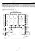
DS3134 SECTION 10: LOCAL BUS 10.1 LOCAL BUS GENERAL DESCRIPTION The Local Bus can operate in two modes, as a PCI Bridge (master mode) and as a Configuration Bus (slave mode). This selection is made in hardware by tying the LMS pin high or low. Figures 10.1A through 10.1C describe the two modes. Figure 10.1A shows an example of the Local Bus being operated in the PCI Bridge Mode. In this example, the Host can access the control ports on the T1/E1 devices via the Local Bus. Figure 10.
DS3134 Bridge Mode Figure 10.1A T1 / E1 Framer or Transceiver DS3134 Chateau PCI / Custom Bus Host Processor and Main Memory T1 / E1 Framer or Transceiver T1 / E1 Framer or Transceiver T1 / E1 Framer or Transceiver lb_cnfga Local Bus Bridge Mode with Arbitration Enabled Figure 10.1B T1 / E1 Framer or Transceiver DS3134 Chateau PCI / Custom Bus T1 / E1 Framer or Transceiver T1 / E1 Framer or Transceiver 1 2 T1 / E1 Framer or Transceiver 3 1. Request Bus Access 2. Bus Access Granted 3.
DS3134 Configuration Mode Figure 10.1C T1 / E1 Framer or Transceiver DS3134 Chateau PCI / Custom Bus No Access Allowed T1 / E1 Framer or Transceiver T1 / E1 Framer or Transceiver Host Processor and Main Memory Only Used to Transfer HDLC Data T1 / E1 Framer or Transceiver lb_cnfgc Local Bus CPU Confgures and Monitors DS3134 Local RAM & ROM PCI Bridge Mode In the PCI Bridge Mode, data from the PCI bus can be transferred to the Local Bus.
DS3134 Local Bus 8-Bit Width Address / LBHE* Setting Table 10.1B PCBE* [3:0] 1110 1101 1011 0111 A1 A0 LBHE* 0 0 1 1 0 1 0 1 1 1 1 1 Note: 1. All other possible states for PCBE* will cause the device to return a Target Abort to the Host. 2. The 8-bit data picked from the PCI bus will be routed/sample to/from the LD[7:0] signal lines. 3. If no PCBE* signals are asserted during an access, a Target Abort is not return and no transaction occurs on the Local Bus.
DS3134 Bridge Mode Bus Arbitration In the Bridge Mode, the Local Bus has the ability to arbitrate for bus access. In order for the feature to operate, the Host must access the PCI Bridge Mode Control Register (LBBMC) and enable it via the LARBE control bit (the default is bus arbitration disabled).
DS3134 Local Bus Access Flowchart Figure 10.
DS3134 10.2 LOCAL BUS BRIDGE MODE CONTROL REGISTER DESCRIPTION Register Name: LBBMC Register Description: Local Bus Bridge Mode Control Register Register Address: 0040h Note: This register can only be accessed via the PCI Bus and hence only in the PCI Bridge Mode. In the Configuration Mode, this register cannot be accessed. It will be set to all zeros upon a hardware reset issued via the PRST* pin.
DS3134 1011 = bus transaction is defined as 11 LCLK periods 1100 = illegal state 1101 = illegal state 1110 = illegal state 1111 = illegal state Bit 6 / Local Bus Width (LBW). 0 = 16 bits 1 = 8 bits Bits 8 to 11 / Local Bus Arbitration Timer Setting (LAT0 to LAT3). These 4 bits determine the total time the Local Bus will seize the bus when it has been granted in the Arbitration Mode (LARBE = 1). This period is measured from LHLDA(LBG*) being detected to LBGACK* inactive.
DS3134 10.3 EXAMPLES OF BUS TIMING FOR LOCAL BUS PCI BRIDGE MODE OPERATION Figure 10.3A 8-Bit Read Cycle Intel Mode (LIM = 0) Arbitration Enabled (LARBE = 1) Bus Transaction Time = 4 LCLK (LRDY = 0100) An attempted access by the Host causes the Local Bus to request the bus.
DS3134 Figure 10.3B 16-Bit Write Cycle Intel Mode (LIM = 0) Arbitration Enabled (LARBE = 1) Bus Transaction Time = 4 LCLK (LRDY = 0100) An attempted access by the Host causes the Local Bus to request the bus. If bus access has not been granted (LBGACK* deasserted), then the timing shown at the top of the page will occur with LHOLD being asserted and then once LHLDA is detected, the Local Bus will grab the bus for 32 to 1048576 clocks and then release it.
DS3134 Figure 10.3C 8-Bit Read Cycle Intel Mode (LIM = 0) Arbitration Disabled (LARBE = 0) Bus Transaction Time = Timed from LRDY* (LRDY = 0000) LCLK LA[19:0] 1 2 3 4 5 6 7 8 9 10 Address Valid LD[7:0] LD[15:8] LBHE* LWR* LRD* LRDY* lb_pi1_V2 10.3C 03/22/99 Note: The LRDY* signal must be detected by the 9th LCLK or the bus access attempted by the Host will be unsuccessful and the LBE status bit will be set.
DS3134 Figure 10.3D 16-Bit Write (only upper 8-bits active) Cycle Intel Mode (LIM = 0) Arbitration Disabled (LARBE = 0) Bus Transaction Time = Timed from LRDY* (LRDY = 0000) LCLK LA[19:0] 1 2 3 4 5 6 7 8 9 10 Address Valid LD[7:0] LD[15:8] Data Valid LBHE* LRD* LWR* LRDY* lb_pi1_v2 10.3D 03/22/99 Note: The LRDY* signal must be detected by the 9th LCLK or the bus access attempted by the Host will be unsuccessful and the LBE status bit will be set.
DS3134 Figure 10.3E 8-Bit Read Cycle Motorola Mode (LIM = 1) Arbitration Enabled (LARBE = 1) Bus Transaction Time = 6 LCLK (LRDY = 0110) An attempted access by the Host causes the Local Bus to request the bus. If bus access has not been granted (LBGACK* deasserted), then the timing shown at the top of the page will occur with LBR* being asserted and then once LBG* is detected, the Local Bus will grab the bus for 32 to 1048576 clocks and then release it.
DS3134 Figure 10.3F 8-Bit Write Cycle Motorola Mode (LIM = 1) Arbitration Enabled (LARBE = 1) Bus Transaction Time = 6 LCLK (LRDY = 0110) An attempted access by the Host causes the Local Bus to request the bus. If bus access has not been granted (LBGACK* deasserted), then the timing shown at the top of the page will occur with LBR* being asserted and then once LBG* is detected, the Local Bus will grab the bus for 32 to 1048576 clocks and then release it.
DS3134 Figure 10.3G 16-Bit Read Cycle Motorola Mode (LIM = 1) Arbitration Disabled (LARBE = 0) Bus Transaction Time = Timed from LRDY* (LRDY = 0000) LCLK LA[19:0] 1 2 3 4 5 6 7 8 9 10 Address Valid LD[7:0] LD[15:8] LBHE* LR/W* LDS* LRDY* lb_pm1_v2 10.3G 03/22/99 Note: The LRDY* signal must be detected by the 9th LCLK or the bus access attempted by the Host will be unsuccessful and the LBE status bit will be set.
DS3134 Figure 10.3H 8-Bit Write Cycle Motorola Mode (LIM = 1) Arbitration Disabled (LARBE = 0) Bus Transaction Time = Timed from LRDY* (LRDY = 0000) LCLK LA[19:0] LD[7:0] 1 2 3 4 5 6 7 8 9 10 Address Valid Data Valid tri-state LD[15:8] LBHE* LR/W* LDS* LRDY* lb_pm1_v2 10.3H\ 03/22/99 Note: The LRDY* signal must be detected by the 9th LCLK or the bus access attempted by the Host will be unsuccessful and the LBE status bit will be set.
DS3134 SECTION 11: JTAG 11.1 JTAG DESCRIPTION The DS3134 device supports the standard instruction codes SAMPLE/PRELOAD, BYPASS, and EXTEST. Optional public instructions included are HIGHZ, CLAMP, and IDCODE. See Figure 11.1A for a Block Diagram. The DS3134 contains the following items, which meet the requirements, set by the IEEE 1149.
DS3134 TAP Controller State Machine Figure 11.2A Test-Logic-Reset 1 0 Run-Test/Idle 1 Select DR-Scan 1 0 1 Select IR-Scan 0 0 1 1 Capture-DR Capture-IR 0 0 Shift-IR Shift-DR 0 0 1 1 1 Exit1-DR 1 Exit1-IR 0 0 Pause-DR Pause-IR 0 0 1 0 0 0 Exit2-DR Exit2-IR 1 1 Update-DR 1 Update-IR 0 1 0 jtag_bd Test-Logic-Reset Upon power-up of the DS3134, the TAP controller will be in the Test-Logic-Reset state. The Instruction register will contain the IDCODE instruction.
DS3134 Capture-DR Data may be parallel loaded into the Test Data registers selected by the current instruction. If the instruction does not call for a parallel load or the selected register does not allow parallel loads, the Test register will remain at its current value. On the rising edge of JTCLK, the controller will go to the Shift-DR state if JTMS is low or it will go to the Exit1-DR state if JTMS is high.
DS3134 Shift-IR In this state, the shift register in the Instruction register is connected between JTDI and JTDO and shifts data one stage for every rising edge of JTCLK towards the serial output. The parallel register, as well as all Test registers remains at their previous states. A rising edge on JTCLK with JTMS high will move the controller to the Exit1-IR state.
DS3134 SAMPLE/PRELOAD A mandatory instruction for the IEEE 1149.1 specification. This instruction supports two functions. The digital I/Os of the DS3134 can be sampled at the Boundary Scan register without interfering with the normal operation of the device by using the Capture-DR state. SAMPLE/PRELOAD also allows the DS3134 to shift data into the Boundary Scan register via JTDI using the Shift-DR state. EXTEST EXTEST allows testing of all interconnections to the DS3134.
DS3134 Boundary Scan Control Bits Table 11.4A Bit Symbol Lead I/O Control Bit Description 213 212 211 210 209 208 207 206 205 204 203 202 201 200 199 198 197 196 195 194 193 192 191 190 189 188 187 186 185 184 183 182 181 180 179 178 177 176 175 174 173 172 171 LD.iocntl LD0 LD1 LD2 LD3 LD4 LD5 LD6 LD7 LD8 LD9 LD10 LD11 LD12 LD13 LD14 LD15 LIM LMS LHOLD(LBR*) LHLDA(LBG*) LBGACK* LINT.iocntl LINT* LCS* LRDY* LCLK LBHE* LWR.iocntl LWR*(LR/W*) LRD.iocntl LRD*(LDS*) LA.
DS3134 Bit Symbol Lead I/O 170 169 168 167 166 165 164 163 162 161 160 159 158 157 156 155 154 153 152 151 150 149 148 147 146 145 144 143 142 141 140 139 138 137 136 135 134 133 132 131 130 129 128 127 126 LA10 LA11 LA12 LA13 LA14 LA15 LA16 LA17 LA18 LA19 RC8 RS8 RD8 TC8 TS8 TD8 RC9 RS9 RD9 TC9 TS9 TD9 RC10 RS10 RD10 TC10 TS10 TD10 RC11 RS11 RD11 TC11 TS11 TD11 RC12 RS12 RD12 TC12 TS12 TD12 RC13 RS13 RD13 TC13 TS13 E18 D19 C20 E17 D18 C19 B20 C18 B19 A20 B17 C17 D16 A18 A17 C16 B16 A16 C15 D14 B15 A1
DS3134 Bit Symbol Lead I/O 125 124 123 122 121 120 119 118 117 116 115 114 113 112 111 110 109 108 107 106 105 104 103 102 101 100 99 98 97 96 95 94 93 92 91 90 89 88 87 86 85 84 83 82 81 TD13 RC14 RS14 RD14 TC14 TS14 TD14 RC15 RS15 RD15 TC15 TS15 TD15 RC0 RS0 RD0 TC0 TS0 TD0 RC1 RS1 RD1 TC1 TS1 TD1 RC2 RS2 RD2 TC2 TS2 TD2 RC3 RS3 RD3 TC3 TS3 TD3 RC4 RS4 RD4 TC4 TS4 TD4 RC5 RS5 C7 B6 A5 D7 C6 B5 A4 C5 B4 A3 D5 C4 B3 B1 C2 D2 D3 E4 C1 D1 E3 E2 E1 F3 G4 F2 F1 G3 G2 G1 H3 H2 H1 J4 J3 J2 J1 M1 M2 M3 N1 N2
DS3134 Bit Symbol Lead I/O 80 79 78 77 76 75 74 73 72 71 70 69 68 67 66 65 64 63 62 61 60 RD5 TC5 TS5 TD5 RC6 RS6 RD6 TC6 TS6 TD6 RC7 RS7 RD7 TC7 TS7 TD7 PRST* PCLK PGNT* PREQ* PAD.iocntl R1 P3 R2 T1 P4 R3 T2 U1 T3 U2 V1 T4 U3 V2 W1 V3 W3 Y2 W4 V4 - I I I O I I I I I O I I I I I O I I I O - 59 58 57 56 55 54 53 52 51 50 49 48 47 46 45 44 43 42 41 40 39 38 37 PAD31 PAD30 PAD29 PAD28 PAD27 PAD26 PAD25 PAD24 PCBE3.iocntl PCBE3* PIDSEL PAD23 PAD22 PAD21 PAD20 PAD19 PAD18 PAD17 PAD16 PCBE2.
DS3134 Bit Symbol Lead I/O Control Bit Description 36 35 34 33 32 PIRDY.iocntl PIRDY* PTRDY.iocntl PTRDY* PDEVSEL.iocntl V10 Y10 - I/O I/O - 0 = PIRDY* is an input; 1 = PIRDY* is an output 31 30 29 28 27 26 25 24 23 22 21 20 19 18 17 16 15 14 13 12 11 10 9 8 7 6 5 4 3 2 1 0 PDEVSEL* PSTOP.iocntl PSTOP* PPERR.iocntl PPERR* PSERR* PPAR.iocntl PPAR PCBE1.iocntl PCBE1* PAD15 PAD14 PAD13 PAD12 PAD11 PAD10 PAD9 PAD8 PCBE0.
DS3134 SECTION 12: AC CHARACTERISTICS ABSOLUTE MAXIMUM RATINGS* Voltage on Any Lead with Respect to VSS (except VDD) Supply Voltage (VDD) with Respect to VSS Operating Temperature Storage Temperature Soldering Temperature -0.3V to 5.5V -0.3V to 3.63V 0C to +70C -55C to +125C See J-STD-020A specification * This is a stress rating only and functional operation of the device at these or any other conditions above those indicated in the operation sections of this specification is not implied.
DS3134 AC CHARACTERISTICS - LAYER ONE PORTS (0°C TO +70°C; VDD = 3.0V TO 3.
DS3134 LAYER ONE PORT AC TIMING DIAGRAM Figure 12A t1 t2 t3 RC[n] / TC[n] Normal Mode RC[n] / TC[n] Inverted Mode t4 t5 RD[n] / RS[n] / TS[n] t6 TD[n] l1 ac Note: TC and RC are independent from each other. In the above timing diagram, all the signals started with “T” are reference to the transmit clock TC and all the signals started with “R” are reference to the receive clock RC. AC CHARACTERISTICS - LOCAL BUS IN BRIDGE MODE (LMS = 0) (0°C TO +70°C; VDD = 3.0V TO 3.
DS3134 LOCAL BUS BRIDGE MODE (LMS = 0) AC TIMING DIAGRAM Figure 12B LCLK t1 LA[19:0] / LD[15:0] / LBHE* / LWR*(LR/W*) / LRD*(DS) Tri-State Data Valid t2 LA[19:0] / LWR*(LR/W*) / LRD*(LDS*) / LBHE* Tri-State Data Valid t3 LA[19:0] / LWR*(LR/W*) / LRD*(DS) / LHOLD(LBR*) / LBGACK* Data Valid t4 t5 t6 t7 LD[15:0] LINT* / LRDY* LHLDA(LBG*) lbus_ac 192 of 203
DS3134 AC CHARACTERISTICS - LOCAL BUS IN CONFIGURATION MODE (LMS = 1) (0°C TO +70°C; VDD = 3.0V TO 3.
DS3134 LOCAL BUS CONFIGURATION MODE (LMS = 1) AC TIMING DIAGRAM Figure 12C Intel Read Cycle t9 LA[15:0] Address Valid Data Valid LD[15:0] t5 LWR* t1 LCS* t2 t3 t4 LRD* LOCAL BUS CONFIGURATION MODE (LMS = 1) AC TIMING DIAGRAM Figure 12C Continued Intel Write Cycle t9 LA[15:0] Address Valid LD[15:0] t7 t8 LRD* t1 LCS* t2 t6 t4 LWR* lb_ac1 194 of 203
DS3134 Motorola Read Cycle t9 LA[15:0] Address Valid Data Valid LD[15:0] t5 LR/W* t1 LCS* t2 t3 t4 LDS* Motorola Write Cycle t9 LA[15:0] Address Valid LD[15:0] t7 t8 LR/W* t1 LCS* t2 t6 t4 LDS* lb_ac1 195 of 203
DS3134 AC CHARACTERISTICS - PCI BUS INTERFACE (0°C TO +70°C; VDD = 3.0V TO 3.
DS3134 AC CHARACTERISTICS - JTAG TEST PORT INTERFACE (0°C TO +70°C; VDD = 3.0V TO 3.
DS3134 SECTION 13: MECHANICAL DIMENSIONS 198 of 203
DS3134 SECTION 14: APPLICATIONS Section 14 describes some possible applications for the DS3134. The number of potential configurations is numerous and only a few are shown. Users are encouraged to contact the factory for support of their particular application. Contact information is shown in Table 14A. Telecom Applications Support Contact Information Table 14A email web telecom.support@dalsemi.com www.dalsemi.
DS3134 QUAD T1/E1 CONNECTION Figure 14C 16 Port T1 or E1 with 256 HDLC Channel Support Figure 14D shows an application where 16 T1 ports are interfaced to a single DS3134. In this application, the T1 lines can be either clear channel or channelized. The DS21Q552 Quad T1 Transceiver performs the line interface function and frames to the T1 line. To convert this application to an E1 design, the DS21Q552 is replaced with the DS21Q554 Quad E1 Transceiver, which is pin-for-pin compatible.
DS3134 Dual T3 with 256 HDLC Channel Support Figure 14E shows an application where two T3 lines are interfaced to a single DS3134. In this application, the T3 lines are demultiplexed by the M13 block and passed to the DS21FF42 Four x Four 16 Channel T1 Framer and DS21FT42 Four x Three 12 Channel T1 Framer devices. The T1 framers locate the frame and multiframe boundaries and interface to the DS3134 by aggregating four T1 lines into a single 8.
DS3134 Single T3 with 512 HDLC Channel Support Figure 14F shows an application where a T3 line is interfaced to two DS3134. In this application, the T3 line is demultiplexed by the M13 block and passed to the DS21FF42 Four x Four 16 Channel T1 Framer and DS21FT42 Four x Three 12 Channel T1 Framer devices. The T1 framers locate the frame and multiframe boundaries and interface to the DS3134. In this application, aggregating four T1 lines into a single 8.
DS3134 Single T3 with 672 HDLC Channel Support Figure 14G shows an application where a T3 line is interfaced to three DS3134. In this application, the T3 line is demultiplexed by the M13 block and passed to the DS21FF42 Four x Four 16 Channel T1 Framer and DS21FT42 Four x Three 12 Channel T1 Framer devices. The T1 framers locate the frame and multiframe boundaries and interface to the DS3134. In this application, aggregating four T1 lines into a single 8.