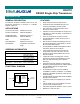
PRODUCT BRIEF DS3170 DS3/E3 Single-Chip Transceiver www.maxim-ic.com GENERAL DESCRIPTION FEATURES The DS3170 combines a DS3/E3 framer and an LIU (single-chip transceiver) to interface to a DS3/E3 physical copper line.
DS3170 DS3/E3 Single-Chip Transceiver DETAILED DESCRIPTION The DS3170 is a software-configured, DS3/E3, single-chip transceiver (SCT). The line interface unit (LIU) has independent receive and transmit paths. The receiver LIU block performs clock and data recovery from a B3ZS- or HDB3-coded AMI signal and monitors for loss of the incoming signal, and can be bypassed for direct clock and data input. The receiver LIU block optionally performs B3ZS/HDB3 decoding.
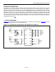
DS3170 DS3/E3 Single-Chip Transceiver TCLKI TSER TSOFI Trail FEAC Trace Buffer PLB HDLC DS3 / E3 Receive Framer B3ZS/ HDB3 Decoder Clock Rate Adapter Serial Interface Mode: SPI (SCLK, MOSI, and MISO) 3 of 233 ROH ROHCLK ROHSOF RDY MODE WIDTH INT GPIO[8:1] CS RD/DS WR/ R/W A[0]/BSWAP A[8:1] D[15:0] RSER RCLKO/RGCLK RSOFO/RDEN UA1 GEN Serial or Parallel uP Inteface RST SPI RX BERT IEEE P1149.
DS3170 DS3/E3 Single-Chip Transceiver TABLE OF CONTENTS 1 BLOCK DIAGRAMS 2 APPLICATIONS 12 FEATURE DETAILS 13 3 3.1 3.2 3.3 3.4 3.5 3.6 3.7 3.8 3.9 3.10 3.11 3.12 3.13 3.14 3.15 2 GLOBAL FEATURES........................................................................................................................................ 13 RECEIVE DS3/E3 LIU FEATURES ..................................................................................................................
DS3170 DS3/E3 Single-Chip Transceiver 9.2.5 Gapped Clocks..................................................................................................................................... 63 9.3 RESET AND POWER-DOWN ............................................................................................................................ 63 9.4 GLOBAL RESOURCES..................................................................................................................................... 66 9.4.
DS3170 DS3/E3 Single-Chip Transceiver 9.11.2 Features ............................................................................................................................................. 108 9.11.3 Configuration and Monitoring ............................................................................................................. 108 9.11.4 Receive Pattern Detection ................................................................................................................. 109 9.11.
DS3170 DS3/E3 Single-Chip Transceiver 17.1 FRAMER DATA PATH AC CHARACTERISTICS ................................................................................................. 220 17.2 OVERHEAD PORT AC CHARACTERISTICS...................................................................................................... 221 17.3 MICRO INTERFACE AC CHARACTERISTICS .................................................................................................... 222 17.3.1 SPI Bus Mode ......................
DS3170 DS3/E3 Single-Chip Transceiver LIST OF FIGURES Figure 1-1. LIU External Connections for the DS3/E3 Port of DS3170 ....................................................................... 2 Figure 1-2. Block Diagram ........................................................................................................................................... 3 Figure 2-1. DS3/E3 Line Card .......................................................................................................................
DS3170 DS3/E3 Single-Chip Transceiver Figure 9-13. DS3 Frame Format................................................................................................................................ 81 Figure 9-14. DS3 Subframe Framer State Diagram .................................................................................................. 81 Figure 9-15. DS3 Multiframe Framer State Diagram................................................................................................. 82 Figure 9-16. G.
DS3170 DS3/E3 Single-Chip Transceiver LIST OF TABLES Table 4-1. Standards Compliance ............................................................................................................................. 16 Table 7-1. DS3170 Short Pin Descriptions ................................................................................................................ 25 Table 7-2. Detailed Pin Descriptions .......................................................................................................
DS3170 DS3/E3 Single-Chip Transceiver Table 11-19. FEAC Receive Side Register Map ..................................................................................................... 165 Table 11-20. Transmit Side Trail Trace Register Map............................................................................................. 168 Table 11-21. Trail Trace Receive Side Register Map.............................................................................................. 169 Table 11-22.
DS3170 DS3/E3 Single-Chip Transceiver 2 APPLICATIONS · · · · · · · · · · · Access Concentrators Multiservice Access Platforms ATM and Frame Relay Equipment Routers and Switches SONET/SDH ADM SONET/SDH Muxes PBXs Digital Cross Connect PDH Multiplexer/Demultiplexer Test Equipment Integrated Access Device (IAD) Figure 2-1 show s a DS3170 application. Figure 2-1.
DS3170 DS3/E3 Single-Chip Transceiver 3 FEATURE DETAILS The following sections describe the features provided by the DS3170 SCT. 3.1 § § § § § § § § § § § 3.2 § § § § § 3.3 § § § § 3.4 § § § § § § § § § § § § Global Features Supports the following transmission formats: C-Bit DS3 M23 DS3 G.751 E3 G.
DS3170 DS3/E3 Single-Chip Transceiver 3.5 § § § § § § § § § § § § 3.6 § § § § § § § 3.7 § § § § § 3.8 § § § § § 3.9 § § § § Transmit DS3/E3 Formatter Features Frame insertion for M23 and C-bit parity DS3, G.751 E3 and G.832 E3 B3ZS/HDB3 encoding Formatter pass-through mode for clear channel applications and externally defined frame formats Generation of RAI, AIS, DS3 idle signal, and G.
DS3170 DS3/E3 Single-Chip Transceiver 3.10 Trail Trace Buffer Features § § § Extraction and storage of the incoming G.832 trail access point identifier in a 16-byte receive register Insertion of the outgoing trail access point identifier from a 16-byte transmit register Receive trace identifier unstable status indication 3.
DS3170 DS3/E3 Single-Chip Transceiver 4 STANDARDS COMPLIANCE Table 4-1. Standards Compliance SPECIFICATION ANSI T1.102-1993 T1.107-1995 T1.231-1997 T1.404-1994 T1.646-1995 ATM Forum af-phy-0034.000 af-phy-0054.
DS3170 DS3/E3 Single-Chip Transceiver 5 ACRONYMS AND GLOSSARY Definition of the terms used in this data sheet: · · · · · · · · · · CCM—Clear-Channel Mode CLAD—Clock Rate Adapter Clear Channel—A Datastream with no framing included, also known as Unframed FRM—Frame Mode FSCT—Framer Single-Chip Transceiver Mode HDLC—High-Level Data-Link Control Packet—HDLC Packet SCT—Single-Chip Transceiver (Framer and LIU) SCT Mode—DS3/E3 Framer and LIU Unchannelized—See Clear Channel 17 of 233
DS3170 DS3/E3 Single-Chip Transceiver 6 MAJOR OPERATIONAL MODES The major operational modes are determined by the FM[2:0] framer mode bits, as well as a few other control bits. Unused features are powered down and the data paths are held in reset. The configuration registers of the unused features can be written to and read from. Some of the IO pins change functions in different operational modes. The line interface operational modes are determined by the LM[2:0] bits. 6.
DS3170 DS3/E3 Single-Chip Transceiver TOH TOHCLK TOHSOF TOHEN Figure 6-1. DS3/E3 Framed LIU Mode TAIS TUA1 TPOS/TDAT TNEG TLCLK DLB Serial Interface Mode: SPI (SCLK, MOSI, and MISO) 19 of 233 ROH ROHCLK ROHSOF RDY MODE WIDTH INT GPIO[8:1] CS RD/DS WR/ R/W A[0]/BSWAP A[8:1] D[15:0] RSER RCLKO/RGCLK RSOFO/RDEN UA1 GEN Serial or Parallel uP Inteface RST SPI RX BERT DS3 / E3 Receive Framer B3ZS/ HDB3 Decoder Clock Rate Adapter REFCLK HDLC IEEE P1149.
DS3170 DS3/E3 Single-Chip Transceiver 6.2 DS3/E3 Unframed LIU Mode The frame mode determines the CLAD clock rate, LIU mode and selects B3ZS or HDB3. FRAME MODE FM[2:0] DS3 Unframed 100 E3 Unframed 110 LIU MODE LM[2:0] TZSD & RZSD TLEN PORT.CR2 JA Off, B3ZS or HDB3 001 0 0 JA RX, B3ZS or HDB3 010 0 0 JA TX, B3ZS or HDB3 011 0 0 JA Off, AMI 001 1 0 JA RX, AMI 010 1 0 JA TX, AMI 011 1 0 Figure 6-2.
DS3170 DS3/E3 Single-Chip Transceiver 6.3 DS3/E3 Framed POS/NEG Mode FRAME MODE FM[2:0] DS3 C-bit Framed 000 DS3 M23 Framed 001 E3 G.751 Framed 010 E3 G.832 Framed 011 LIU MODE LM[2:0] TLEN PORT.CR2 TZSD & RZSD LIU Off, B3ZS or HDB3 000 0 1 LIU Off, AMI 000 1 1 TOH TOHCLK TOHSOF TOHEN Figure 6-3.
DS3170 DS3/E3 Single-Chip Transceiver 6.4 DS3/E3 Unframed POS/NEG Mode The frame mode determines the CLAD clock rate if used as the transmit clock and selects B3ZS or HDB3. FRAME MODE FM[2:0] DS3 Unframed 100 E3 Unframed 110 LIU MODE LM[2:0] TZSD & RZSD TLEN PORT.CR2 LIU Off, B3ZS or HDB3 000 0 1 LIU Off, AMI 000 1 1 Figure 6-4.
DS3170 DS3/E3 Single-Chip Transceiver 6.5 DS3/E3 Framed UNI Mode FRAME MODE FM[2:0] DS3 C-bit Framed 000 DS3 M23 Framed 001 E3 G.751 Framed 010 E3 G.832 Framed 011 LIU MODE LM[2:0] Unipolar Mode TLEN PORT.CR2 TZSD & RZSD 1XX X 1 TOH TOHCLK TOHSOF TOHEN Figure 6-5.
DS3170 DS3/E3 Single-Chip Transceiver 6.6 DS3/E3 Unframed UNI Mode The frame mode determines the CLAD clock rate if used as the transmit clock. FRAME MODE FM[2:0] DS3 Unframed 100 E3 Unframed 110 LIU MODE LM[2:0] Unipolar Mode TZSD & RZSD 1XX X TLEN PORT.CR2 1 Figure 6-6.
DS3170 DS3/E3 Single-Chip Transceiver 7 PIN DESCRIPTIONS Note: In JTAG mode, all digital pins are bidirectional to increase the effectiveness of board level ATPG patterns for isolation of interconnect failures. 7.1 Short Pin Descriptions Table 7-1.
DS3170 DS3/E3 Single-Chip Transceiver NAME TYPE D[2]/SPI_SCLK D[1]/SPI_MOSI IO IO D[0]SPI_MISO IO A[8] A[7] A[6] A[5] A[4] A[3] A[2] A[1] A[0]/BSWAP ALE CS RD/DS I I I I WR / R/W RDY INT MODE WIDTH SPI I Oz O I I I GPIO[8] GPIO[7] GPIO[6] GPIO[5] GPIO[4] GPIO[3] GPIO[2] GPIO[1] TEST HIZ RST IO JTCLK JTMS JTDI JTDO JTRST I Ipu Ipu Oz Ipu Data [2] / SPI Serial Interface Clock < 10 MHz Data [1] / SPI Serial Interface Data Master-out Slave-in Data [0] / SPI Serial Interface Data Master-in Slave-o
DS3170 DS3/E3 Single-Chip Transceiver NAME TYPE AVSSR AVSST AVSSJ AVSSC PWR PWR PWR PWR UNUSED1 UNUSED2 7.2 N/A N/A FUNCTION Analog Gnd for Receive LIU Analog Gnd for Transmit LIU Analog Gnd for Jitter Attenuator Analog Gnd for CLAD UNUSED Unused Unused PIN BGA B5 E4 D2 G1 LQFP 92 14 10 19 D6 G2 89 20 Detailed Pin Descriptions Table 7-2.
DS3170 DS3/E3 Single-Chip Transceiver TYPE PIN DESCRIPTION TNEG PIN NAME O TXP Oa TXN Oa RXP Ia RXN Ia RLCLK I Transmit Negative AMI / Line OH Mask TNEG: When the port line is configured for B3ZS, HDB3 or AMI mode and the transmit line interface pins are enabled (PORT.CR2.TLEN), a high on this pin indicates that a negative pulse should be transmitted on the line.
DS3170 DS3/E3 Single-Chip Transceiver TYPE PIN DESCRIPTION RPOS / RDAT PIN NAME Iad RNEG / RLCV Iad Receive Positive AMI / Data RPOS: When the port line is configured for B3ZS, HDB3 or AMI mode and the LIU is disabled, a high on this pin indicates that a positive pulse has been detected using an external LIU. The signal is sampled on the positive clock edge of the referenced clock pin if the clock pin signal is not inverted, otherwise it is sampled on the falling edge of the clock.
DS3170 DS3/E3 Single-Chip Transceiver TYPE PIN DESCRIPTION TOHCLK PIN NAME O TOHSOF O ROH O ROHCLK O ROHSOF O TCLKI I Transmit Overhead Clock TOHCLK: When the port framer is configured for one of the DS3 or E3 framing modes, this clock is used for the transmit overhead port signals TOH, TOHEN and TOHSOF. The TOHSOF output signal is updated and the TOH and TOHEN input signals are sampled at the same time this clock signal transitions from high to low.
DS3170 DS3/E3 Single-Chip Transceiver TYPE PIN DESCRIPTION TSOFI PIN NAME I TSER I TCLKO / TGCLK O Transmit Start Of Frame Input See Table 9-20. TSOFI: This signal can be used to align the start of the DS3 or E3 frames on the TSER pin to an external signal. In framed modes, the TSOFI signal can be used to align the start of frame signal position on the TSER/TOH pin to the rising edge of a signal on this pin. The signal edge does not need to occur on every frame and can be tied high or low.
DS3170 DS3/E3 Single-Chip Transceiver TYPE PIN DESCRIPTION TSOFO / TDEN PIN NAME O RSER O RCLKO / RGCLK O RSOFO / RDEN O Framer Start Of Frame / Data Enable See Table 9-21. TSOFO: When the port framer is configured for the DS3 or E3 framed modes and the TSOFO pin function is selected, this signal is used to indicate the start of the DS3/E3 frame on the TSER pin. This signal pulses high three clocks before the first overhead bit in a DS3 or E3 frame that will be input on TSER.
DS3170 DS3/E3 Single-Chip Transceiver PIN NAME TYPE D[15:8] IO D[7]/ SPI_CPOL IO D[6]/ SPI_CPHA IO D[5]/ SPI_SWAP IO D[4:3] IO D[2]/ SPI_SCLK IO D[1]/ SPI_MOSI IO D[0]/ SPI_MISO IO A[8:1] I A[0] / BSWAP ALE I PIN DESCRIPTION positions of the data on the RSER pin. The signal goes high during each DS3/E3 payload bit and goes low during each DS3/E3 overhead bit.
DS3170 DS3/E3 Single-Chip Transceiver PIN NAME TYPE CS I RD / DS I WR / R/W I RDY Oz INT Oz MODE I WIDTH I SPI I GPIO1 IO GPIO2 IO GPIO3 IO GPIO4 IO GPIO5 IO GPIO6 IO GPIO7 IO PIN DESCRIPTION address systems. When it is high the address is fed through the address latch to the internal logic. When it transitions to low, the address is latched and held internally until the signal goes back high. ALE should be tied high for nonmultiplexed address systems.
DS3170 DS3/E3 Single-Chip Transceiver PIN NAME GPIO8 TYPE IO TEST I HIZ I RST I JTCLK I JTMS Ipu JTDI Ipu JTDO Oz JTRST Ipu PIN DESCRIPTION GPIO7: This signal is configured to be a general purpose IO pin. General Purpose IO 8 GPIO8: This signal is configured to be a general purpose IO pin, or the PMU input signal. When configured for PMU input, the signal low time and high time must be greater than 500 nsec.
DS3170 DS3/E3 Single-Chip Transceiver PIN NAME AVSSR AVSST AVSSJ AVSSC TYPE PWR PWR PWR PWR PIN DESCRIPTION Analog Ground for receive LIU Analog Ground for transmit LIU Analog Ground for jitter attenuator Analog Ground for CLAD 36 of 233
DS3170 DS3/E3 Single-Chip Transceiver 7.3 Pin Functional Timing 7.3.1 Line IO 7.3.1.1 B3ZS/HDB3/AMI Mode Transmit Pin Functional Timing There is no suggested time alignment between the TXP, TXN and TX LINE signals and the TLCLK clock signal. The TX DATA signal is not a readily available signal, it is meant to represent the data value of the other signals. The TXP and TXN signals are only available when the line is in B3ZS/HDB3 or AMI mode and the LIU is enabled.
DS3170 DS3/E3 Single-Chip Transceiver Figure 7-2. Tx Line IO HDB3 Functional Timing Diagram TLCLK (TX DATA) TPOS TNEG B TXP V B V B V B V BIAS V TXN 0V (TX LINE) + - HDB3 CODEWORD 7.3.1.2 B3ZS/HDB3/AMI Mode Receive Pin Functional Timing There is no suggested time alignment between the RXP, RXN and RX LINE signals and the RLCLK clock signal. The RX DATA signal is not an always readily available signal, it is meant to represent the data value of the other signals.
DS3170 DS3/E3 Single-Chip Transceiver Figure 7-4. Rx Line IO HDB3 Functional Timing Diagram RLCLK (RX DATA) RPOS RNEG B RXP V B V B V B V BIAS V RXN 0V (RX LINE) + - HDB3 CODEWORD 7.3.1.
DS3170 DS3/E3 Single-Chip Transceiver Figure 7-6. Rx Line IO UNI Functional Timing Diagram RLCLK RDAT RLVC INC BPV COUNTER TWICE 7.3.2 INC BPV COUNTER ONCE DS3/E3 Framing Overhead Functional Timing Figure 7-7 shows the relationship between the DS3 receive overhead port pins. Figure 7-7.
DS3170 DS3/E3 Single-Chip Transceiver Figure 7-10 shows the relationship between the DS3 transmit overhead port pins. Figure 7-10. DS3 Framing Transmit Overhead Port Timing TOHCLK TOHSOF TOHEN TOH F73 C73 F74 1 2 3 X1 4 F11 5 C11 F12 C12 F13 6 7 8 9 C13 10 F14 11 X2 12 F21 13 C21 14 F22 15 C22 16 F23 17 C23 18 F24 19 P1 20 F31 C31 F32 23 C32 21 22 24 FAS 6 FAS 8 FAS 9 FAS 9 21 22 23 24 Figure 7-11 shows the relationship between the E3 G.
DS3170 DS3/E3 Single-Chip Transceiver Figure 7-13. DS3 Framed Mode Transmit Serial Interface Pin Timing TCLKO or TCLKI TSOFO TSOFI DS3 TGCLK DS3 TSER DS3 TDEN TSER DATA IS OVERWRITTEN WITH OH 1 2 3 4 5 6 7 8 9 10 11 12 13 14 15 Figure 7-14. E3 G.751 Framed Mode Transmit Serial Interface Pin Timing TCLKO or TCLKI TSOFO TSOFI E3 TGCLK TSER DATA IS OVERWRITTEN WITH OH E3 TSER E3 TDEN 1 2 3 4 5 6 7 8 9 10 11 12 13 14 15 Figure 7-15. E3 G.
DS3170 DS3/E3 Single-Chip Transceiver Figure 7-16. DS3 Framed Mode Receive Serial Interface Pin Timing RCLKO or RCLKI RSOFO DS3 RGCLK DS3 RSER X1 DS3 RDEN 1 2 3 4 5 6 7 8 9 10 11 12 13 14 15 Figure 7-17. E3 G.751 Framed Mode Receive Serial Interface Pin Timing RCLKO or RCLKI RSOFO E3 RGCLK FAS 1111010000 A N 14 15 E3 RSER E3 RDEN 1 2 3 4 5 6 7 8 9 10 11 12 13 Figure 7-18. E3 G.
DS3170 DS3/E3 Single-Chip Transceiver expected. If the BURST bit is not set, each data byte will be followed by the control byte(s) for the next access. Additionally, CS may also be de-asserted between accesses when CPHA =1. In the case, any BURST access is terminated, and the next byte received when CS is re-asserted will be a control byte. The following diagrams describe the functionality of the SPI port for the four combinations of SPI_CPOL and SPI_CPHA.
DS3170 DS3/E3 Single-Chip Transceiver Figure 7-23. SPI Serial Port Access For Write Mode, SPI_CPOL = 0, SPI_CPHA = 0 SCK CS* MOSI 0 A13 A12 A11 A10 A9 A8 MSB A7 A6 LSB MSB A5 A4 A3 A2 A1 A0 B D7 LSB MSB D6 D5 D4 D3 D2 D1 D0 LSB MISO Figure 7-24. SPI Serial Port Access For Write Mode, SPI_CPOL = 1, SPI_CPHA = 0 SCK CS* MOSI 0 A13 A12 A11 A10 A9 A8 MSB A7 A6 LSB MSB A5 A4 A3 A2 A1 A0 B D7 LSB MSB D6 D5 D4 D3 D2 D1 D0 LSB MISO Figure 7-25.
DS3170 DS3/E3 Single-Chip Transceiver Figure 7-27. 16-Bit Mode Write A[0]/BSWAP 0x2B0 A[10:1] D[15:0] 0x1234 CS WR RD RDY Z Z Note: Address 0x2B0 = 0x1234 Figure 7-28.
DS3170 DS3/E3 Single-Chip Transceiver Figure 7-29. 8-Bit Mode Write A[0]/BSWAP A[10:1] D[7:0] 0x2B0 0x2B0 0x34 0x12 CS WR RD RDY Z Z Z Z Note: Address 0x2B0 = 0x34 0x2B1 = 012 Figure 7-30. 8-Bit Mode Read A[0]/BSWAP 0x2B0 0x2B0 A[10:1] D[7:0] 0x12 0x34 CS WR RD RDY Z Z Z Z Note: Address 0x2B0 = 0x34 0x2B1 = 012 Figure 7-31 and Figure 7-32 are examples of databuses without and with byte swapping enabled, respectively.
DS3170 DS3/E3 Single-Chip Transceiver Figure 7-31. 16-Bit Mode without Byte Swap A[0]/BSWAP 0x2B0 A[10:1] D[15:0] 0x2B2 0x1234 0x5678 CS WR RD RDY Z Z Z Z Note: Address 0x2B0 = 0x1234 0x2B2 = 0x5678 Figure 7-32b 16-Bit Mode with Byte Swap A[0]/BSWAP 0x2B2 0x2B0 A[10:1] D[15:0] 0x3412 0x7856 CS WR RD RDY Z Z Z Z Note: Address 0x2B0 = 0x1234 0x2B2 = 0x5678 Clearing status latched registers on a read or write access is selectable via the GL.CR1.LSBCRE register bit.
DS3170 DS3/E3 Single-Chip Transceiver Figure 7-33. Clear Status Latched Register on Read A[0]/BSWAP 0x1C0 A[10:1] D[15:0] 0x1C0 0xFFFF 0x0000 CS WR RD RDY Z Z Z Z Figure 7-34.
DS3170 DS3/E3 Single-Chip Transceiver Figure 7-35. RDY Signal Functional Timing Write A[0]/BSWAP A[10:1] D[15:0] 0x2B0 0x3A4 0x1234 0x0078 CS WR RD RDY Z Z Z Z Figure 7-36. RDY Signal Functional Timing Read A[0]/BSWAP 0x1C0 A[10:1] D[15:0] 0x3A4 0xFFFF 0xFFFF CS WR RD RDY Z Z Z See also Figure 17-8 and Figure 17-9. 7.3.5 JTAG Functional Timing See Section 12.5.
DS3170 DS3/E3 Single-Chip Transceiver 8 INITIALIZATION AND CONFIGURATION STEP 1: Check Device ID Code. Before any testing can be done, the device ID code, which is stored in GL.IDR, shoud be checked against the device ID code shown below to ensure correct device is being used. Current device ID codes is: o DS3170 rev 1.0: 004Fh STEP 2: Initialize the Device.
DS3170 DS3/E3 Single-Chip Transceiver Table 8-1. Configuration of Port Register Settings PORT.CR1 0x040 PORT.CR2 0x042 PORT.CR3 0x044 PORT.CR4 0x046 DS3 C-Bit Framed 0x2000 0000 0011 0000 0111 0x0000 0x0000 DS3 M13 Framed 0x2000 0000 0011 0000 1111 0x0000 0x0000 E3.751 Framed 0x2000 0000 0011 0001 0111 0x0000 0x0000 E3.
DS3170 DS3/E3 Single-Chip Transceiver 9 FUNCTIONAL DESCRIPTION 9.1 9.1.1 Processor Bus Interface SPI Serial Port Mode The external processor bus can be configured to operate in SPI serial bus mode. See the section 7.3.4.1 for detailed timing diagrams. When SPI = 1, SPI bus mode is implemented using four signals: clock (CLK), master-out slave-in data (MOSI), master-in slave-out data (MISO), and chip select (CS). Clock polarity and phase can be set by the D[7]/SPI_CPOL and D[6]/SPI_CPHA pins.
DS3170 DS3/E3 Single-Chip Transceiver The clear on write mode expects the user to use the following protocol: 1. Read the latched status register 2. Write to the registers with the bits set that need to be cleared. This protocol is useful when multiple uncoordinated software tasks access the same latched register. Each task should only clear the bits with which it is concerned; the other tasks will clear the bits with which they are concerned.
DS3170 DS3/E3 Single-Chip Transceiver Figure 9-1. Interrupt Structure SRL bit SRIE bit SRL bit PORT.ISR bit SRIE bit SRL bit GL.ISR.PISRn SRIE bit GL.ISRIE. PISRIEn BLOCK LATCHED STATUS and INTERRUPT ENABLE REGISTERS PORT INTERRUPT STATUS REGISTER GLOBAL INTERRUPT STATUS REGISTER and INTERRUPT ENABLE REGISTER PORT INTERRUPTS INT GLOBAL INTERRUPTS Figure 9-1 not only tells the user how to determine which event caused the interrupt, it also tells the user how to enable a particular interrupt.
DS3170 DS3/E3 Single-Chip Transceiver 9.2.1.1.1 LIU Enabled, Loop Timing Enabled In this mode, the receive LIU sources the clock for both the receive and transmit logic. The RCLKO, TCLKO and TLCLK clock output pins will be the same. The transmit or receive line payload signal pins can be timed to any of these clock. The use of the RCLKO pin as the timing source is suggested. If RCLKO is used as the timing source, be sure to set PORT.CR3.RFTS = 0 for output timing. 9.2.1.1.
DS3170 DS3/E3 Single-Chip Transceiver 9.2.2 Sources of Clock Output Pin Signals The clock output pins can be sourced from many clock sources. The clock sources are the transmit input clocks pin (TCLKI), the receive clock input pin (RLCLK), the recovered clock in the receive LIU, and the clock signals in the clock rate adapter circuit (CLAD).
DS3170 DS3/E3 Single-Chip Transceiver Table 9-3 identifies the source of the output signal TLCLK based on certain variables and register bits. Table 9-3. Source Selection of TLCLK Clock Signal SIGNAL TLCLK LOOPT (PORT. CR3) LBM[2:0] (PORT.CR4) LLB or PLB LIUEN CLADC (PORT.
DS3170 DS3/E3 Single-Chip Transceiver Table 9-4. Source Selection of TCLKO (Internal Tx Clock) SIGNAL LOOPT PORT.CR3 LBM[2:0] (PORT.CR4) LIUEN CLADC (PORT.CR3) SOURCE TCLKO 1 1 0 0 0 0 XXX XXX PLB (011) PLB (011) PLB disabled PLB disabled 1 0 1 0 X X X X X X 0 1 Rx LIU RLCLK Rx LIU RLCLK CLAD TCLKI Figure 9-3 shows the source of the RCLKO signals. Figure 9-3.
DS3170 DS3/E3 Single-Chip Transceiver 9.2.3.1 Transmit Line Interface Pins Timing Source Selection (TPOS/TDAT, TNEG) The transmit line interface signal pin group has the same functional timing clock source as the TLCLK pin described in Table 9-3. Other clock pins can be used for the external timing. The TLCLK transmit line clock output pin is always a valid output clock for external logic to use for these signals when PORT.CR3.TLTS=0.
DS3170 DS3/E3 Single-Chip Transceiver LOOPT LBM[2:0] LIUEN CLADC TFTS Table 9-7.
DS3170 DS3/E3 Single-Chip Transceiver 0 0 0 0 0 0 0 0 9.2.4 RFTS 0 XXX XXX XXX PLB (011) or DLB (100) or ALB (001) PLB (011) or DLB (100) DLB&LLB (110) LLB (010) not LLB, DLB or PLB (00X) DLB (100) or LLB & DLB (110) DLB (100) or LLB & DLB (110) not DLB (100) and not LLB & DLB (110) not DLB (100) and not LLB & DLB (110) CLADC 1 1 1 LBM[2:0] LIUEN LOOPT Table 9-9.
DS3170 DS3/E3 Single-Chip Transceiver Figure 9-4.
DS3170 DS3/E3 Single-Chip Transceiver reset values. The processor bus output signals are also forced to be HIZ when the RST pin is active (low). The global reset bit (GL.CR1.RST) stays set after a one is written to it, but is reset to zero when the external RST pin is active or when a zero is written to it. At the port level, the global reset signal combines with the port reset bit in the port control register (PORT.CR1.RST) to create a port reset signal.
DS3170 DS3/E3 Single-Chip Transceiver Table 9-10.
DS3170 DS3/E3 Single-Chip Transceiver 9.4 9.4.1 Global Resources Clock Rate Adapter (CLAD) The clock rate adapter is composed of a PLL block to create the internal clock which can be used for the transmit clock and/or LIU reference clock from a clock input on the reference input (REFCLK) pin. The device needs one of two (DS3 or E3) internal clock rates. The input reference clock frequency can be either 44.736, 34.368. 77.78, 51.84 or 19.44 MHz. The receive LIU is supplied a reference clock from the CLAD.
DS3170 DS3/E3 Single-Chip Transceiver Table 9-12. Global 8 kHz Reference Source Table GL.CR2. G8KIS 0 0 0 0 1 GL.CR2. G8KRS[1:0] 00 01 10 11 XX SOURCE None, the 8KHZ divider is disabled. Derived from CLAD output clock 8KREF source selected by P8KRS[1:0] Undefined GPIO4 Table 9-13 lists the selectable sources for port 8 kHz reference sources. Table 9-13. Port 8 kHz Reference Source Table PORT.CR3.
DS3170 DS3/E3 Single-Chip Transceiver 9.4.4 General-Purpose IO Pins There are eight general-purpose IO pins that can be used for general IO, global signals and framer alarm signals. Each pin is independently configurable to be a general-purpose input, general-purpose output, global signal or framer alarm. Two of the GPIO pins can be programmed to output one or two framer alarm statuses. One of the two pins assigned to framer alarms can be programmed as global input or output signals.
DS3170 DS3/E3 Single-Chip Transceiver 0000 0001 0010 0011 0100 0101 0110 0111 1000 1001 1010 1011 1100 1101 1110 1111 9.4.5 DS3 IDLE DS3/E3 RAI DS3/E3 AIS DS3/E3 LOF DS3/E3 OOF PORT.CR4 GPIO(A/B)[3:0] LINE LOS Table 9-16. GPIO Port Alarm Monitor Select X X X X X X X X X X X X X X X X X X X X Performance Monitor Counter Update Details The performance monitor counters are designed to count at least one second of events before saturating to the maximum count.
DS3170 DS3/E3 Single-Chip Transceiver Figure 9-7. Performance Monitor Update Logic PORT.CR1.PMUM other port counters PORT.CR1.PMU GL.CR1.GPMU GPIO8(GPMU) PIN ONE SEC GL.SR.GPMS 0 PMU 00 01 1X 1 PMS PERF COUNTER PORT.SR.PMS GTZ GL.CR1.GPM 9.4.6 Transmit Manual Error Insertion Transmit errors can be inserted in some of the functional blocks. These errors can be inserted using register bits in the functional blocks, using the global GL.CR1.TMEI bit, using the port PORT.CR1.
DS3170 DS3/E3 Single-Chip Transceiver Figure 9-8. Transmit Error Insert Logic BERT.TEICR.MEIMS BERT.TEICR error insertion bit 0 PORT.CR.MEIMS 1 0 PORT.CR.TMEI BERT ERROR INSERT T3.TEIR.MEIMS GL.CR1.MEIMS 1 GL.CR1.TMEI 0 GPIO6 PIN (TMEI) 1 T3.TEIR error insertion bit 0 1 T3 ERROR INSERT 0 1 9.5 Port Resources 9.5.1 Loopbacks There are several loop back paths available.
DS3170 DS3/E3 Single-Chip Transceiver Figure 9-9 highlights where each loopback mode is located and gives an overall view of the various loopback paths available. Figure 9-9. Loopback Modes TAIS TUA1 DS3/E3 Receive LIU DS3 / E3 Transmit Formatter TX BERT HDLC RX BERT DS3 / E3 Receive Framer B3ZS/ HDB3 Decoder IEEE P1149.1 JTAG Test Access Port Clock Rate Adapter 9.5.1.
DS3170 DS3/E3 Single-Chip Transceiver 9.5.1.2 Line Loopback (LLB) Line loopback is enabled by setting PORT.CR4.LBM[2:0] = X10. DLB and LLB are enabled at the same time when LBM[2:0] = 110, and only LLB is enabled when LBM[2:0] = 010. The clock from the receive LIU or the RLCLK pin will be output to the transmit LIU or TCLKO pin. The POS and NEG data from the receive LIU or the RPOS and RNEG pin will be sampled with the receive clock to time it to the LIU or pin interface.
DS3170 DS3/E3 Single-Chip Transceiver The sequence will only work when the automatic AIS generation is not enabled. CV and P-bit errors can occur when AIS is automatically generated and can not be avoided. This sequence to generate an error free DS# AIS at the top level is to have the DS3 AIS or unframed all ones signal initiate in the DS3 framer, and a few frames sent before initiating or terminating the DS3 AIS or unframed all ones at the top level.
DS3170 DS3/E3 Single-Chip Transceiver Table 9-18 lists the LAIS decodes for various line AIS enable modes. Table 9-18. Line AIS Enable Modes LAIS[1:0] PORT.CR1 FRAME MODE DESCRIPTION AIS CODE DS3 Automatic AIS when DLB is enabled (PORT.CR4.LBM = 1XX) DS3AIS 00 E3 Automatic AIS when DLB is enabled UA1 01 Any Send UA1 UA1 10 DS3 Send AIS DS3AIS 10 E3 Send AIS UA1 11 Any Disable none 00 Table 9-19 lists the PAIS decodes for various payload AIS enable modes. Table 9-19.
DS3170 DS3/E3 Single-Chip Transceiver long. The generated BERT signal replaces the data on the TSER pin in framed modes when the BERT is enabled by setting the PORT.CR1.BENA. When the BERT is enabled The TDEN and RDEN pins will still be active but the data on the TSER pin will be discarded. 9.5.8 System Port Pins The system port pins have multiple functions based on the framing mode the device is in as well as other pin mode select bits. 9.5.8.
DS3170 DS3/E3 Single-Chip Transceiver Table 9-23. RSOFO/RDEN Output Pin Functions FM[2:0] PORT.CR2 RSOFOS PORT.CR3 PIN FUNCTION 0XX (FRM) 0 RDEN 0XX (FRM) 1 RSOFO 1XX (UFRM) X High Table 9-24. RCLKO/RGCLK Output Pin Functions FM[2:0] PORT.CR2 RCLKS PORT.CR3 PIN FUNCTION GAP SOURCE 0XX (FRM) 0 RGCLK RDEN 0XX (FRM) 1 RCLKO none 1XX (UFRM) X RCLKO none 9.5.9 Framing Modes The framing modes are selected independently of the line interface modes using the PORT.CR2.
DS3170 DS3/E3 Single-Chip Transceiver Table 9-26. Line Mode Select Bits LM[2:0] LINE.TCR.TZSD & LINE.RCR.RZSD LM[2:0] (PORT.
DS3170 DS3/E3 Single-Chip Transceiver 9.6 DS3/E3 Framer / Formatter 9.6.1 General Description The Receive DS3/E3 Framer receives a unipolar DS3/E3 signal, determines frame alignment and extracts the DS3/E3 overhead in the receive direction. The Transmit DS3/E3 Formatter receives a DS3/E3 payload, generates framing, inserts DS3/E3 overhead, and outputs a unipolar DS3/E3 signal in the transmit direction.
DS3170 DS3/E3 Single-Chip Transceiver · · · · · · Arbitrary framing format support – Accepts a signal with an arbitrary framing format. The Line overhead/stuff periods are removed from the data stream using an overhead mask signal. Detects alarms and errors – Detects DS3 alarm conditions (SEF, OOMF, OOF, LOF, COFA, AIS, AIC, RDI, and Idle) and errors (framing, parity, and FEBE), or E3 alarm conditions (OOF, LOF, COFA, AIS, and RDI/RAI) and errors (framing, parity, and REI).
DS3170 DS3/E3 Single-Chip Transceiver Figure 9-13. DS3 Frame Format X1 F11 C11 F12 C12 F13 C13 F14 X2 F21 C21 F22 C22 F23 C23 F24 P1 F31 C31 F32 C32 F33 C33 F34 P2 F41 C41 F42 C42 F43 C43 F44 M1 F51 C51 F52 C52 F53 C53 F54 M2 F61 C61 F62 C62 F63 C63 F64 M3 F71 C71 F72 C72 F73 C73 F74 7 SubFrames 680 Bits The subframe framer continually searches four adjacent bit positions for a subframe boundary.
DS3170 DS3/E3 Single-Chip Transceiver boundary. The multiframe boundary is found by identifying the three multiframe alignment bits (M-bits). Since there are seven multiframe bits and three bits are required to identify the multiframe boundary, up to 9 checks may be needed to find the multiframe boundary. Once the multiframe boundary is identified, it is checked in each subsequent frame.
DS3170 DS3/E3 Single-Chip Transceiver A Loss Of Frame (LOF) condition is declared by the LOF integration counter when it has been active for a total of T ms. The LOF integration counter is active (increments count) when an OOF condition is present, it is inactive (holds count) when an OOF condition is absent, and it is reset when an OOF condition is absent for T continuous ms. T is programmable (0, 1, 2, or 3). An LOF condition is terminated when an OOF condition is absent for T continuous ms.
DS3170 DS3/E3 Single-Chip Transceiver FEBE errors (C-bit format only) are determined by the C-bits in subframe four (C41, C42, and C43). A value of 111 indicates no error and any other value indicates an error. The receive alarm indication (RAI) bit will be set high in the transmitter when one or more of the indicated alarm conditions is present, and low when all of the indicated alarm conditions are absent.
DS3170 DS3/E3 Single-Chip Transceiver Table 9-27.
DS3170 DS3/E3 Single-Chip Transceiver The bits C31, C32, and C33 are all overwritten with the calculated payload parity from the previous DS3 frame. The bits C41, C42, and C43 are all overwritten with the Far-End Block Error (FEBE) bit. The FEBE bit can be generated automatically or inserted from a register bit. The FEBE bit source is programmable (automatic or register). If the FEBE bit is generated automatically, it is zero when at least one C-bit parity error has been detected during the previous frame.
DS3170 DS3/E3 Single-Chip Transceiver 9.6.5.5.1 Receive C-bit DS3 Frame Format The DS3 frame format is shown in Figure 9-13. X1 and X2 are the Remote Defect Indication (RDI) bits (also referred to as the far-end SEF/AIS bits). P1 and P2 are the parity bits used for line error monitoring. M1, M2, and M3 are the multiframe alignment bits that define the multiframe boundary. FXY are the subframe alignment bits that define the subframe boundary. Note: Both the M-bits and F-bits define the DS3 frame boundary.
DS3170 DS3/E3 Single-Chip Transceiver more of the indicated alarm conditions is present, and set to one when all of the indicated alarm conditions are absent. Automatically setting RDI on LOS, SEF, LOF, or AIS is individually programmable (on or off). The P-bits (P1 and P2) are both overwritten with the calculated payload parity from the previous DS3 frame. The payload parity is calculated by performing modulo 2 addition of all of the payload bits after all frame processing has been completed.
DS3170 DS3/E3 Single-Chip Transceiver 9.6.6.5.1 Receive M23 DS3 Frame Format The DS3 frame format is shown in Figure 9-13. The X1 and X2 are the Remote Defect Indication (RDI) bits (also referred to as the far-end SEF/AIS bits). P1 and P2 are the parity bits used for line error monitoring. M1, M2, and M3 are the multiframe alignment bits that define the multiframe boundary. FXY are the subframe alignment bits that define the subframe boundary.
DS3170 DS3/E3 Single-Chip Transceiver Once all of the E3 overhead bits have been overwritten, the data stream is passed on to error insertion. If frame generation is disabled, the incoming E3 signal is passed on directly to error insertion. Frame generation is programmable (on or off). 9.6.7.3 Transmit G.751 E3 Error Insertion Error insertion inserts framing errors into the frame alignment signal (FAS). The type of error(s) inserted into the FAS is programmable (errored FAS bit or errored FAS).
DS3170 DS3/E3 Single-Chip Transceiver A Change Of Frame Alignment (COFA) is declared when the G.751 E3 framer updates the data path frame counters with a frame alignment that is different from the current data path frame alignment. A Loss Of Signal (LOS) condition is declared when the HDB3 encoder is active, and it declares an LOS condition. An LOS condition is terminated when the HDB3 encoder is inactive, or it terminates an LOS condition.
DS3170 DS3/E3 Single-Chip Transceiver Figure 9-17. G.832 E3 Frame Format FA1 FA2 EM TR MA NR 530 Byte Payload GC 59 Columns Figure 9-18. MA Byte Format MSB 1 RDI LSB 8 REI SL SL SL MI MI TM RDI - Remote Defect Indicator REI - Remote Error Indicator SL - Signal Label MI - Multi-frame Indicator TM - Timing Marker Table 9-29 shows the function of each overhead bit in the DS3 Frame. Table 9-29. G.
DS3170 DS3/E3 Single-Chip Transceiver FA1 and FA2 are the Frame Alignment bytes. EM is the Error Monitoring byte used for path error monitoring. TR is the Trail Trace byte used for end-to-end connectivity verification. MA is the Maintenance and Adaptation byte used for far-end path status and performance monitoring. NR is the Network Operator byte allocated for network operator maintenance purposes. GC is the General Purpose Communications Channel byte allocated for user communications purposes. 9.6.8.
DS3170 DS3/E3 Single-Chip Transceiver The type of BIP-8 error(s) inserted is programmable (errored BIP-8 bit, or errored BIP-8 byte). An errored BIP-8 bit is inverting a single bit error in the EM byte. An errored BIP-8 byte is inverting all eight bits in the EM byte. BIP-8 error(s) can be inserted one error at a time, or continuously. The BIP-8 error insertion mode (single or continuous) is programmable. An REI error is generated by forcing the second bit of the MA byte to a one.
DS3170 DS3/E3 Single-Chip Transceiver A Change Of Frame Alignment (COFA) is declared when the G.832 E3 framer updates the data path frame counters with a frame alignment that is different from the current data path frame alignment. A Loss Of Signal (LOS) condition is declared when the HDB3 encoder is active, and it declares an LOS condition. An LOS condition is terminated when the HDB3 encoder is inactive, or it terminates an LOS condition.
DS3170 DS3/E3 Single-Chip Transceiver Table 9-30. Payload Label Match Status EXPECTED RECEIVED STATUS 000 000 Match 000 001 Mismatch 000 XXX Mismatch 001 000 Mismatch 001 001 Match 001 XXX Match XXX 000 Mismatch XXX 001 Match XXX XXX Match XXX YYY Mismatch XXX and YYY equal any value other than 000 or 001; XXX ¹ YYY.
DS3170 DS3/E3 Single-Chip Transceiver The bits in a byte are received MSB first, LSB last. When they are output serially, they are output MSB first, LSB last. The bits in a byte in an incoming signal are numbered in the order they are received, 1 (MSB) to 8 (LSB). However, when a byte is stored in a register, the MSB is stored in the lowest numbered bit (0), and the LSB is stored in the highest numbered bit (7). This is to differentiate between a byte in a register and the corresponding byte in a signal.
DS3170 DS3/E3 Single-Chip Transceiver 9.7.4 Transmit HDLC Overhead Processor The Transmit HDLC Overhead Processor accepts data from the Transmit FIFO, performs bit reordering, FCS processing, stuffing, packet abort sequence insertion, and inter-frame padding. A byte is read from the Transmit FIFO with a packet end status.
DS3170 DS3/E3 Single-Chip Transceiver number of bits between the end flag and the start flag will be an integer number of bytes (flags). Any time there is less than 16 bits between two flags, the data will be discarded. Packet abort detection searches for a packet abort sequence. Between a packet start flag and a packet end flag, if an abort sequence is detected, the packet is marked with an abort indication, and all subsequent data is discarded until a packet start flag is detected.
DS3170 DS3/E3 Single-Chip Transceiver The Trail Trace Controller extracts/inserts E3-G.832 trail access point identifiers using a 16-byte register(one for transmit, one for receive). The Trail Trace Controller demaps a 16-byte trail trace identifier from the E3-G.832 datastream in the receive direction and maps a trace identifier into the E3-G.832 datastream in the transmit direction.
DS3170 DS3/E3 Single-Chip Transceiver order they are received, 1 (MSB) to 8 (LSB). However, when a byte is stored in a register, the MSB is stored in the highest numbered bit (7), and the LSB is stored in the lowest numbered bit (0). This is to differentiate between a byte in a register and the corresponding byte in a signal. 9.8.4 Transmit Data Storage The Transmit Data Storage block contains memory for 16 bytes of data and controller circuitry for reading and writing the memory.
DS3170 DS3/E3 Single-Chip Transceiver Figure 9-21. Trail Trace Byte (DT = Trail Trace Data) Bit 1 MSB Bit 2 Bit 3 Bit 4 Bit 5 Bit 6 Bit 7 Bit 8 LSB MAS or DT[1] DT[2] DT[3] DT[4] DT[5] DT[6] DT[7] DT[8] Trail trace extraction extracts the trail trace identifier from the incoming trail trace data stream, generates a trail trace identifier change indication, detects a trail trace identifier idle (Idle) condition, and detects a trail trace identifier unstable (TIU) condition.
DS3170 DS3/E3 Single-Chip Transceiver The transmit direction inputs codewords from the microprocessor via the register interface and stores the codewords. It removes the codewords and performs FEAC processing. See Figure 9-22 for the location of the FEAC Controller in the block diagram Figure 9-22. FEAC Controller Block Diagram TAIS TUA1 DLB · · · · TX BERT HDLC RX BERT DS3 / E3 Receive Framer B3ZS/ HDB3 Decoder Clock Rate Adapter 9.9.
DS3170 DS3/E3 Single-Chip Transceiver have both been sent ten times, all ones are output. In continuous mode, the code from TFCA[5:0] is inserted into a codeword, and sent until the mode is changed 9.9.3.3 Receive FEAC Processor The Receive FEAC Processor accepts an incoming data line and extracts all overhead and performs FEAC code extraction , and Idle detection. Figure 9-23.
DS3170 DS3/E3 Single-Chip Transceiver Figure 9-24. Line Encoder/Decoder Block Diagram TAIS TUA1 DLB Trail FEAC Trace Buffer TX BERT HDLC PLB LLB ALB DS3/E3 Receive LIU DS3 / E3 Transmit Formatter B3ZS/ HDB3 Encoder DS3/E3 Transmit LIU B3ZS/ HDB3 Decoder Clock Rate Adapter RX BERT DS3 / E3 Receive Framer IEEE P1149.1 JTAG Test Access Port UA1 GEN Microprocessor Interface 9.10.
DS3170 DS3/E3 Single-Chip Transceiver as the values for the first one. The third bipolar one is generated according to the normal AMI rules. When an EXZ error is to be inserted, the Transmit Line Interface waits for the next occurrence of three (four) consecutive zeros on the bipolar signal, and inhibits the insertion of a B3ZS (HDB3) signature. There must be at least one intervening one between consecutive BPV or EXZ errors.
DS3170 DS3/E3 Single-Chip Transceiver Figure 9-25. B3ZS Signatures RLCLK (RX DATA) RPOS V RNEG B3ZS SIGNATURE WHEN LINE.RCR.RZSF = 0 RLCLK (RX DATA) RPOS V V RNEG B3ZS SIGNATURE WHEN LINE.RCR.RZSF = 1 Figure 9-26. HDB3 Signatures RLCLK (RX DATA) RPOS RNEG V HDB3 SIGNATURE WHEN LINE.RCR.RZSF = 0 RLCLK (RX DATA) RPOS RNEG V V HDB3 SIGNATURE WHEN LINE.RCR.RZSF = 1 BPV detection checks the bipolar signal for bipolar violation (BPV) errors and E3 code violation (CV) errors.
DS3170 DS3/E3 Single-Chip Transceiver 9.11 BERT 9.11.1 General Description The BERT is a software programmable test pattern generator and monitor capable of meeting most error performance requirements for digital transmission equipment. It will generate and synchronize to pseudo-random n y patterns with a generation polynomial of the form x + x + 1, where n and y can take on values from 1 to 32 and to repetitive patterns of any length up to 32 bits.
DS3170 DS3/E3 Single-Chip Transceiver Table 9-31. Pseudo-Random Pattern Generation PATTERN TYPE 9 2 -1 O.153 (511 type) 11 2 -1 O.152 and O.153 (2047 type) 15 2 -1 O.151 BERT.CR BERT.PCR Register PTF[4:0] PLF[4:0] PTS (hex) (hex) 04 08 0 BERT. PCR 0x0408 QRSS 0 08 0A 0 0 0x080A BERT. SPR2 0xFFFF BERT.
DS3170 DS3/E3 Single-Chip Transceiver then checking the next 32 data stream bits. Synchronization is achieved if all 32 bits match the incoming pattern. If at least six incoming bits in the current 64-bit window do not match the receive pattern generator, automatic pattern resynchronization is initiated. Automatic pattern resynchronization can be disabled. Refer to Figure 9-28 for the PRBS synchronization diagram. Figure 9-28.
DS3170 DS3/E3 Single-Chip Transceiver Figure 9-29. Repetitive Pattern Synchronization State Diagram Sync f6 err ors 6o 32 ors err bi t sw ith h wit its out 4b 1 bit error Verify Match Pattern Matches 9.11.4.3 Receive Pattern Monitoring Receive pattern monitoring monitors the incoming data stream for both an OOS condition and bit errors and counts the incoming bits. An Out Of Synchronization (OOS) condition is declared when the synchronization state machine is not in the “Sync” state.
DS3170 DS3/E3 Single-Chip Transceiver 9.12 LIU – Line Interface Unit 9.12.1 General Description The line interface units (LIUs) perform the functions necessary for interfacing at the physical layer to DS3 or E3 lines. The LIU has independent receive and transmit paths and a built-in jitter attenuator. See Figure 9-30 for the location within the DS3170 device of the LIU. Figure 9-30.
DS3170 DS3/E3 Single-Chip Transceiver waveforms onto 75W coaxial cable. Refer to Figure 9-31 for a detailed functional block diagram of the DS3/E3 LIU. The jitter attenuator can be mapped into the receiver data path, mapped into the transmitter data path, or be disabled. The DS3/E3 LIU conforms to the telecommunications standards listed in Table 4-1. Figure 1-1 shows the external components required for proper operation. Figure 9-31.
DS3170 DS3/E3 Single-Chip Transceiver 9.12.4.3 Interfacing to the Line The transmitter interfaces to the outgoing DS3/E3 coaxial cable (75W) through a 2:1 step-down transformer connected to the TXP and TXN pins. Figure 1-1 shows the arrangement of the transformer and other recommended interface components. Table 9-33 specifies the required characteristics of the transformer. 9.12.4.4 Transmit Driver Monitor If the transmit driver monitor detects a faulty transmitter, it sets the PORT.SR.TDM status bit.
DS3170 DS3/E3 Single-Chip Transceiver Table 9-34. Recommended Transformers PART TEMP RANGE PIN-PACKAGE/ SCHEMATIC OCL PRIMARY (mH) (min) LL (mH) (max) BANDWIDTH 75W (MHz) Pulse Engineering PE-65968 0°C to +70°C 6 SMT LS-1/C 19 0.06 0.250 to 500 Pulse Engineering PE-65969 0°C to +70°C 19 0.06 0.250 to 500 19 0.06 0.250 to 500 19 0.06 0.
DS3170 DS3/E3 Single-Chip Transceiver The ALOS detector in the AGC/equalizer block detects that the incoming signal is less than or equal to a signal level approximately 24dB below nominal, and mutes the data coming out of the clock and data recovery block. (24dB below nominal in the “tolerance range” of G.775, where LOS may or may not be declared.
DS3170 DS3/E3 Single-Chip Transceiver 10 OVERALL REGISTER MAP The register addresses of the global, test and the port are concatenated to cover the address range of 000 to 7FF. The address map requires 9 bits of address, ADR[8:0]. The register banks that are not marked with an “X” are not writeable and read back all zeroes. Bits that are underlined are read-only; all other bits are read-write. Unused bits and registers marked with “—“ are ignored when written to, and return zero when read.
DS3170 DS3/E3 Single-Chip Transceiver Address offset Description 08C – 08F B3ZS/HDB3 transmit line encoder 090 – 09F B3ZS/HDB3 receive line decoder 0A0 – 0AF HDLC Transmit 0B0 – 0BF HDLC Receive 0C0 – 0CF FEAC Transmit 0D0 – 0DF FEAC Receive 0E0 – 0E7 Unused 0E8 – 0EF Trail Trace Transmit 0F0 – 0FF Trail Trace Receive 100 – 117 Unused 118 – 11F DS3/E3 Framer Transmit 120 – 13F DS3/E3 Framer Receive 140 – 17F Unused 180 – 19F Test Registers 1A0 – 1FF Unused 118 of 233
DS3170 DS3/E3 Single-Chip Transceiver 11 REGISTER MAPS AND DESCRIPTIONS 11.1 Registers Bit Maps Note: In 8-bit mode, register bits[15:8] correspond to the upper byte, and register bits[7:0] correspond to the lower byte. For example, address 001h is the upper byte (bits [15:8]) and address 000h is the lower byte (bits [7:0]) for register GL.IDR in 8-bit mode. All registers listed, including those designated Unused and Reserved, will cause the RDY signal to go low when written to or read from.
DS3170 DS3/E3 Single-Chip Transceiver Address 16-bit 8-bit 040 040 041 042 042 043 044 044 045 046 046 047 048 048 049 04A 04A 04B 04C 04C 04D 04E 04E 04F 050 050 051 052 052 053 054 054 055 056 056 057 058- 05805E 05F Register Type Bit 7 Bit 15 PORT.CR1 RW PORT.CR2 RW PORT.CR3 RW PORT.CR4 RW UNUSED PORT.INV1 RW PORT.INV2 RW UNUSED PORT.ISR R PORT.SR R PORT.SRL RL PORT.
DS3170 DS3/E3 Single-Chip Transceiver Address 16-bit 8-bit 074 074 075 076 076 077 078 078 079 07A 07A 07B 07C- 07C 07E 07F Register Type Bit 7 Bit 15 BERT.RBECR1 R BERT.RBECR2 R BERT.RBCR1 R BERT.
DS3170 DS3/E3 Single-Chip Transceiver Address 16-bit 8-bit 0AA- 0AA 0AE 0AF 0B0 0B0 0B1 0B2 0B2 0B3 0B4 0B4 0B5 0B6 0B6 0B7 0B8 0B8 0B9 0BA 0BA 0BB 0BC 0BC 0BD 0BE 0BE 0BF Register Type Bit 7 Bit 15 UNUSED HDLC.RCR RW UNUSED HDLC.RSR R HDLC.RSRL RL HDLC.RSRIE RW UNUSED HDLC.
DS3170 DS3/E3 Single-Chip Transceiver Table 11-7. Trail Trace Register Bit Map Address 16-bit 8-bit 0E8 0E8 0E9 0EA 0EA 0EB 0EC 0EC 0ED 0EE 0EE 0EF 0F0 0F0 0F1 0F2 0F2 0F3 0F4 0F4 0F5 0F6 0F6 0F7 0F8 0F8 0F9 0FA 0FA 0FB 0FC 0FC 0FD 0FE 0FE 0FF 100- 100116 1117 Register Type Bit 7 Bit 15 TT.TCR RW TT.TTIAR R TT.TIR R UNUSED TT.RCR RW TT.RTIAR R TT.RSR R TT.RSRL RL TT.RSRIE RW UNUSED TT.RIR R TT.
DS3170 DS3/E3 Single-Chip Transceiver Address 16-bit 8-bit 12A 12A 12B 12C 12C 12D 12E 12E 12F 130- 130 132 133 134 134 135 136 136 137 138 138 139 13A 13A 13B 13C- 13C 13E 13F 11.1.4 Register Type Bit 7 Bit 15 T3.RSRL2 RL T3.RSRIE1 RW T3.RSRIE2 RW RESERVED T3.RFECR R T3.RPECR R T3.RFBECR R T3.
DS3170 DS3/E3 Single-Chip Transceiver Address Register 16-bit 8-bit 136- 136RESERVED 13A 13B 13C- 13CUNUSED 13E 13F 11.1.5 Type Bit 7 Bit 15 Bit 6 Bit 14 ----- Bit 5 Bit 13 ----- ----- Bit 4 Bit 12 ----- Bit 3 Bit 11 ----- Bit 2 Bit 10 ----- Bit 1 Bit 9 Bit 0 Bit 8 ----- ----- Bit 1 Bit 9 Bit 0 Bit 8 E3 G.832 Register Bit Map Table 11-10. E3 G.
DS3170 DS3/E3 Single-Chip Transceiver 11.2 Global Registers Table 11-11.
DS3170 DS3/E3 Single-Chip Transceiver GL.CR1 Global Control Register 1 002h Register Name: Register Description: Register Address: Bit # Name Default 15 13 0 14 INTM 0 0 12 -0 Bit # Name Default 7 TMEI 0 6 MEIMS 0 5 GPM1 0 4 GPM0 0 -- -- 11 0 10 -0 9 -0 8 -0 3 PMU 0 2 LSBCRE 0 1 RSTDP 1 0 RST 0 -- Bit 14: INT pin mode (INTM) This bit determines the inactive mode of the INT pin. The INT pin always drives low when active.
DS3170 DS3/E3 Single-Chip Transceiver GL.CR2 Global Control Register 2 004h Register Name: Register Description: Register Address: Bit # Name Default 15 -0 14 -0 13 -0 12 -0 11 G8KRS1 0 10 G8KRS0 0 9 G8K0S 0 8 G8KIS 0 Bit # Name Default 7 -0 6 -0 5 -0 4 -0 3 CLAD2 0 2 CLAD1 0 1 CLAD0 0 0 -0 Bits 11 to 10: Global 8KHz Reference Source [1:0] (G8KRS[1:0]).
DS3170 DS3/E3 Single-Chip Transceiver Register Name: Register Description: Register Address: GL.GIOCR Global General Purpose IO Control Register 00Ah Bit # Name Default 15 GPIO8S1 0 14 GPIO8S0 0 13 GPIO7S1 0 12 GPIO7S0 0 11 GPIO6S1 0 10 GPIO6S0 0 9 GPIO5S1 0 8 GPIO5S0 0 Bit # Name Default 7 GPIO4S1 0 6 GPIO4S0 0 5 GPIO3S1 0 4 GPIO3S0 0 3 GPIO2S1 0 2 GPIO2S0 0 1 GPIO1S1 0 0 GPIO1S0 0 Bits 15 to 14: General Purpose IO 8 Select [1:0] (GPIO8S[1:0]).
DS3170 DS3/E3 Single-Chip Transceiver Bits 1 to 0: General Purpose IO 1 Select [1:0] (GPIO1S[1:0]). These bits determine the function of the GPIO1 pin. 00 = Input 01 = Port A status output selected by PORT.CR4:GPIOA[3:0] in port control registers 10 = Output logic 0 11 = Output logic 1 GL.
DS3170 DS3/E3 Single-Chip Transceiver GL.SR Global Status Register 014h Register Name: Register Description: Register Address: Bit # Name 15 -- 14 -- 13 -- 12 -- 11 -- 10 -- 9 -- 8 -- Bit # Name 7 -- 6 -- 5 -- 4 -- 3 -- 2 -- 1 CLOL 0 GPMS Bit 1 : CLAD Loss of Lock (CLOL) – This bit is set when any of the PLLs in the CLAD are not locked to the reference frequency.
DS3170 DS3/E3 Single-Chip Transceiver GL.SRIE Global Status Register Interrupt Enable 018h Register Name: Register Description: Register Address: Bit # Name Default 15 -0 14 -0 13 -0 12 -0 11 -0 10 -0 9 -0 8 -0 Bit # Name Default 7 -0 6 -0 5 -0 4 -0 3 -0 2 ONESIE 0 1 CLOLIE 0 0 GPMSIE 0 Bit 2: One Second Interrupt Enable (ONESIE) This bit will drive the interrupt pin low if the GL.SRL.ONESL bit is set, and the GL.ISRIE.GSRIE bit is enabled.
DS3170 DS3/E3 Single-Chip Transceiver 11.3 Port Register 11.3.1 Register Bit Descriptions Table 11-12. Port Register Map Address 040h 042h 044h 046h 048h 04Ah 04Ch 04Eh 050h 052h 054h 056h 058h 05Ah 05Ch 05Eh Register PORT.CR1 PORT.CR2 PORT.CR3 PORT.CR4 -PORT.INV1 PORT.INV2 -PORT.ISR PORT.SR PORT.SRL PORT.
DS3170 DS3/E3 Single-Chip Transceiver PORT.CR1 Port Control Register 1 040h Register Name: Register Description: Register Address: Bit # Name Default RESERVED 15 13 PAIS1 0 12 PAIS0 0 11 LAIS1 0 10 LAIS0 0 9 BENA 0 RESERVED 0 14 PAIS2 0 Bit # Name Default 8 7 TMEI 0 6 MEIM 0 5 --- 4 PMUM 0 3 PMU 0 2 PD 1 1 RSTDP 1 0 RST 0 0 Bits 14 to 12: Payload AIS Select [2:0] (PAIS[2:0]).
DS3170 DS3/E3 Single-Chip Transceiver 1 = Transmit BERT logic enabled Bit 7: Transmit Manual Error Insert (TMEI) This bit is used to insert errors in all error insertion logic configured to use this bit when PORT.CR1.MEIM=0. The error(s) will be inserted when this bit is toggled low to high. Bit 6 : Transmit Manual Error Insert Mode (MEIM). These bits select the method transmit manual error insertion for this port for error generators configured to use the external TMEI signal.
DS3170 DS3/E3 Single-Chip Transceiver 0 = TXP and TXN driven 1 = TXP and TXN tri-stated Bit 13: Receive LIU Monitor Mode (RMON) This bit is used to enable the receive LIU monitor mode pre-amplifier. Enabling the pre-amplifier adds about 20 dB of linear amplification for use in monitor applications where the signal has been reduced 20 dB using resistive attenuator circuits.
DS3170 DS3/E3 Single-Chip Transceiver PORT.CR3 Port Control Register 3 044h Register Name: Register Description: Register Address: Bit # Name Default 15 -0 14 -0 13 RCLKS 0 12 RSOFOS 0 RESERVED 11 9 TSOFOS 0 RESERVED 0 10 TCLKS 0 Bit # Name Default 7 P8KRS1 0 6 P8KRS0 0 5 P8KREF 0 4 LOOPT 0 8 3 CLADC 0 2 RFTS 0 1 TFTS 0 0 TLTS 0 0 Bit 13: Receive Clock Output Select (RCLKS). This bit is used to select the function of the RGCLK / RCLKO pins. See Table 9-24.
DS3170 DS3/E3 Single-Chip Transceiver Bit 2: Receive Framer IO Signal Timing Select (RFTS). This bit controls the timing reference for the signals on the receive framer interface IO pins. The pins controlled are RSER, RSOFO / RDEN. See Table 9-8 for more details. 0 = Use output clocks for timing reference 1 = Use input clocks for timing reference Bit 1: Transmit Framer IO Signal Timing Select (TFTS). This bit controls the timing reference for the signals on the transmit framer interface IO pins.
DS3170 DS3/E3 Single-Chip Transceiver 0000 0001 0010 0011 0100 0101 0110 0111 1000 1001 1010 1011 1100 1101 1110 1111 DS3 IDLE DS3/E3 RAI DS3/E3 AIS DS3/E3 LOF DS3/E3 OOF PORT.CR4 GPIO(A/B)[3:0] LINE LOS Table 9-16.
DS3170 DS3/E3 Single-Chip Transceiver PORT.INV1 Port IO Invert Control Register 1 04Ah Register Name: Register Description: Register Address: Bit # Name Default 15 14 RESERVED RESERVED 12 TSOFOI 0 RESERVED 0 13 -0 0 Bit # Name Default 7 TOHI 0 11 0 10 TSERI 0 9 TOHSI 0 8 TOHEI 0 6 TOHCKI 0 5 TSOFII 0 4 TNEGI 0 3 TDATI 0 2 TLCKI 0 1 TCKOI 0 0 TCKII 0 Bit 12 : TSOFO / TDEN/ Invert (TSOFOI). This bit inverts the TSOFO / TDEN pin when set. Bit 10 : TSER Invert (TSERI).
DS3170 DS3/E3 Single-Chip Transceiver PORT.ISR Port Interrupt Status Register 050h Register Name: Register Description: Register Address: Bit # Name 15 -- 14 -- 13 -- 12 -- 11 -- 10 -- 9 Bit # Name 7 TTSR 6 FSR 5 HSR 4 BSR 3 2 1 RESERVED RESERVED RESERVED PSR 8 LCSR 0 FMSR Bit 9: Port Status Register Interrupt Status (PSR) This bit is set when any of the latched status register bits, that are enabled for interrupt, in the PORT.SRL register are set.
DS3170 DS3/E3 Single-Chip Transceiver Bit 1: Receive Loss Of Lock Status (RLOL) This bits indicates the status of the receive LIU clock recovery PLL circuit. 0 = Locked to the incoming signal 1 = Not locked to the incoming signal Bit 0: Performance Monitoring Update Status (PMS) This bits indicates the status of all active performance monitoring register and counter update signals in this port.
DS3170 DS3/E3 Single-Chip Transceiver Bit 1: Receive Loss Of Lock Latched Status Interrupt Enable (RLOLIE) The interrupt pin will be driven when this bit is enabled and the PORT.SRL.RLOLL bit is set and the bit in GL.ISRIE.PISRIE bit is enabled. Bit 0: Performance Monitoring Update Latched Status Interrupt Enable (PMSIE) The interrupt pin will be driven when this bit is enabled and the PORT.SRL.PMSL bit is set and the bit in GL.ISRIE.PISRIE bit is enabled.
DS3170 DS3/E3 Single-Chip Transceiver 11.4 BERT 11.4.1 BERT Register Map The BERT utilizes twelve registers. Table 11-13. BERT Register Map Address 060h 062h 064h 066h 068h 06Ah 06Ch 06Eh 070h 072h 074h 076h 078h 07Ah 07Ch 07Eh Register Register Description BERT.CR BERT.PCR BERT.SPR1 BERT.SPR2 BERT.TEICR -BERT.SR BERT.SRL BERT.SRIE -BERT.RBECR1 BERT.RBECR2 BERT.RBCR1 BERT.
DS3170 DS3/E3 Single-Chip Transceiver must be changed to zero and back to one for another pattern to be loaded. Loading a new pattern will forces the receive pattern generator out of the “Sync” state which causes a resynchronization to be initiated. Note: QRSS, PTS, PLF[4:0}, PTF[4:0], and BSP[31:0] must not change from the time this bit transitions from 0 to 1 until four receive clock cycles after this bit transitions from 0 to 1.
DS3170 DS3/E3 Single-Chip Transceiver BERT.SPR1 BERT Seed/Pattern Register #1 064h Register Name: Register Description: Register Address: Bit # Name Default 15 BSP15 0 14 BSP14 0 13 BSP13 0 12 BSP12 0 11 BSP11 0 10 BSP10 0 9 BSP9 0 8 BSP8 0 Bit # Name Default 7 BSP7 0 6 BSP6 0 5 BSP5 0 4 BSP4 0 3 BSP3 0 2 BSP2 0 1 BSP1 0 0 BSP0 0 Bits 15 to 0: BERT Seed/Pattern (BSP[15:0]) – Lower sixteen bits of 32 bits. Register description follows next register. BERT.
DS3170 DS3/E3 Single-Chip Transceiver TEIR[2:0] Error Rate 000 Disabled 001 1*10 -1 010 1*10 -2 011 1*10 -3 100 1*10 -4 101 1*10 -5 110 1*10 -6 111 1*10 -7 Bit 2: Bit Error Insertion Enable (BEI) – When 0, single bit error insertion is disabled. When 1, single bit error insertion is enabled.
DS3170 DS3/E3 Single-Chip Transceiver BERT.SRL BERT Status Register Latched 06Eh Register Name: Register Description: Register Address: Bit # Name 15 -- 14 -- 13 -- 12 -- 11 -- 10 -- 9 -- 8 -- Bit # Name 7 -- 6 -- 5 -- 4 -- 3 PMSL 2 BEL 1 BECL 0 OOSL Bit 3: Performance Monitoring Update Status Latched (PMSL) – This bit is set when the PMS bit transitions from 0 to 1. Bit 2: Bit Error Latched (BEL) – This bit is set when a bit error is detected.
DS3170 DS3/E3 Single-Chip Transceiver BERT.RBECR1 BERT Receive Bit Error Count Register #1 074h Register Name: Register Description: Register Address: Bit # Name Default 15 BEC15 0 14 BEC14 0 13 BEC13 0 12 BEC12 0 11 BEC11 0 10 BEC10 0 9 BEC9 0 8 BEC8 0 Bit # Name Default 7 BEC7 0 6 BEC6 0 5 BEC5 0 4 BEC4 0 3 BEC3 0 2 BEC2 0 1 BEC1 0 0 BEC0 0 Bits 15 to 0: Bit Error Count (BEC[15:0]) – Lower sixteen bits of 24 bits. Register description follows next register. BERT.
DS3170 DS3/E3 Single-Chip Transceiver BERT.RBCR1 Receive Bit Count Register #1 078h Register Name: Register Description: Register Address: Bit # Name Default 15 BC15 0 14 BC14 0 13 BC13 0 12 BC12 0 11 BC11 0 10 BC10 0 9 BC9 0 8 BC8 0 Bit # Name Default 7 BC7 0 6 BC6 0 5 BC5 0 4 BC4 0 3 BC3 0 2 BC2 0 1 BC1 0 0 BC0 0 Bits 15 to 0: Bit Count (BC[15:0]) – Lower sixteen bits of 32 bits. Register description follows next register. BERT.
DS3170 DS3/E3 Single-Chip Transceiver 11.5 B3ZS/HDB3 Line Encoder/Decoder 11.5.1 Transmit Side Line Encoder/Decoder Register Map The transmit side utilizes one register. Table 11-14. Transmit Side B3ZS/HDB3 Line Encoder/Decoder Register Map Address 08Ch 08Eh Register LINE.TCR -- Register Description Line Transmit Control Register Unused 11.5.1.1 Register Bit Descriptions LINE.
DS3170 DS3/E3 Single-Chip Transceiver 11.5.2 Receive Side Line Encoder/Decoder Register Map The receive side utilizes six registers. Table 11-15. Receive Side B3ZS/HDB3 Line Encoder/Decoder Register Map Address 090h 092h 094h 096h 098h 09Ah 09Ch 09Eh Register LINE.RCR -LINE.RSR LINE.RSRL LINE.RSRIE -LINE.RBPVCR LINE.
DS3170 DS3/E3 Single-Chip Transceiver Bit 0: Receive Zero Suppression Decoding Disable (RZSD) – When 0, the B3ZS/HDB3 Decoder performs zero suppression (B3ZS or HDB3) and AMI decoding. When 1, zero suppression (B3ZS or HDB3) decoding is disabled, and only AMI decoding is performed. LINE.RSR Line Receive Status Register (0.2.4.
DS3170 DS3/E3 Single-Chip Transceiver LINE.RSRIE Line Receive Status Register Interrupt Enable (0.2.4.6)98h Register Name: Register Description: Register Address: Bit # Name Default 15 -0 14 -0 13 -0 12 -0 11 -0 10 -0 9 -0 8 -0 Bit # Name Default 7 -0 6 -0 5 ZSCDIE 0 4 EXZIE 0 3 EXZCIE 0 2 BPVIE 0 1 BPVCIE 0 0 LOSIE 0 Bit 5: Zero Suppression Code Detect Interrupt Enable (ZSCDIE) – This bit enables an interrupt if the LINE.RSRL.ZSCDL bit is set and the bit in GL.ISRIE.
DS3170 DS3/E3 Single-Chip Transceiver LINE.REXZCR Line Receive Excessive Zero Count Register (0.2.4.
DS3170 DS3/E3 Single-Chip Transceiver 11.6 HDLC 11.6.1 HDLC Transmit Side Register Map The transmit side utilizes five registers. Table 11-16. Transmit Side HDLC Register Map Address 0A0h 0A2h 0A4h 0A6h 0A8h 0AAh 0ACh 0AEh Register HDLC.TCR HDLC.TFDR HDLC.TSR HDLC.TSRL HDLC.
DS3170 DS3/E3 Single-Chip Transceiver Bit 1: Transmit FCS Processing Disable (TFPD) – This bit controls whether or not an FCS is calculated and appended to the end of each packet. When 0, the calculated FCS bytes are appended to the end of the packet. When 1, the packet is transmitted without an FCS. Bit 0: Transmit FIFO Reset (TFRST) – When 0, the Transmit FIFO will resume normal operations, however, data is discarded until a start of packet is received after RAM power-up is completed.
DS3170 DS3/E3 Single-Chip Transceiver HDLC.TSRL HDLC Transmit Status Register Latched 0A6h Register Name: Register Description: Register Address: Bit # Name 15 -- 14 -- 13 -- 12 -- 11 -- 10 -- 9 -- 8 -- Bit # Name 7 -- 6 -- 5 TFOL 4 TFUL 3 TPEL 2 -- 1 TFEL 0 THDAL Bit 5: Transmit FIFO Overflow Latched (TFOL) – This bit is set when a Transmit FIFO overflow condition occurs. Bit 4: Transmit FIFO Underflow Latched (TFUL) – This bit is set when a Transmit FIFO underflow condition occurs.
DS3170 DS3/E3 Single-Chip Transceiver Bit 2: Transmit FIFO Full Interrupt Enable (TFFIE) – This bit enables an interrupt if the TFFL bit is set and the bit in GL.ISRIE.PSRIE[4:1] that corresponds to this port is set. 0 = interrupt disabled 1 = interrupt enabled Bit 1: Transmit FIFO Empty Interrupt Enable (TFEIE) – This bit enables an interrupt if the TFEL bit is set and the bit in GL.ISRIE.PSRIE[4:1] that corresponds to this port is set.
DS3170 DS3/E3 Single-Chip Transceiver Bit 0: Receive FIFO Reset (RFRST) – When 0, the Receive FIFO will resume normal operations, however, data is discarded until a start of packet is received after RAM power-up is completed. When 1, the Receive FIFO is emptied, any transfer in progress is halted, the FIFO RAM is powered down, the RHDA bit is forced low, and all incoming data is discarded. HDLC.
DS3170 DS3/E3 Single-Chip Transceiver HDLC.RSRIE HDLC Receive Status Register Interrupt Enable 0B8h Register Name: Register Description: Register Address: Bit # Name Default 15 -0 14 -0 13 -0 12 -0 11 -0 10 -0 9 -0 8 -0 Bit # Name Default 7 RFOIE 0 6 -0 5 -0 4 RPEIE 0 3 RPSIE 0 2 RFFIE 0 1 -0 0 RHDAIE 0 Bit 7: Receive FIFO Overflow Interrupt Enable (RFOIE) – This bit enables an interrupt if the RFOL bit is set and the bit in GL.ISRIE.PSRIE[4:1] that corresponds to this port is set.
DS3170 DS3/E3 Single-Chip Transceiver Bits 3 to 1: Receive Packet Status (RPS[2:0]) – These three bits indicate the status of the received packet and packet data. 000 = packet middle 001 = packet start. 010 = reserved 011 = reserved 100 = packet end: good packet 101 = packet end: FCS errored packet. 110 = packet end: invalid packet (a noninteger number of bytes). 111 = packet end: aborted packet.
DS3170 DS3/E3 Single-Chip Transceiver 11.7 FEAC Controller 11.7.1 FEAC Transmit Side Register Map The transmit side utilizes five registers. Table 11-18. FEAC Transmit Side Register Map Address 0C0h 0C2h 0C4h 0C6h 0C8h 0CAh 0CCh 0CEh Register FEAC.TCR FEAC.TFDR FEAC.TSR FEAC.TSRL FEAC.
DS3170 DS3/E3 Single-Chip Transceiver FEAC.TFDR Transmit FEAC Data Register 0C2h Register Name: Register Description: Register Address: Bit # Name Default 15 -0 14 -0 13 TFCB5 0 12 TFCB4 0 11 TFCB3 0 10 TFCB2 0 9 TFCB1 0 8 TFCB0 0 Bit # Name Default 7 -0 6 -0 5 TFCA5 0 4 TFCA4 0 3 TFCA3 0 2 TFCA2 0 1 TFCA1 0 0 TFCA0 0 Bits 13 to 8: Transmit FEAC Code B (TFCB[5:0]) – These six bits are the transmit FEAC code B data to be stored inserted into codeword B.
DS3170 DS3/E3 Single-Chip Transceiver FEAC.TSRIE FEAC Transmit Status Register Interrupt Enable 0C8h Register Name: Register Description: Register Address: Bit # Name Default 15 -0 14 -0 13 -0 12 -0 11 -0 10 -0 9 -0 8 -0 Bit # Name Default 7 -0 6 -0 5 -0 4 -0 3 -0 2 -0 1 -0 0 TFIIE 0 Bit 0: Transmit FEAC Idle Interrupt Enable (TFIIE) – This bit enables an interrupt if the TFIL bit is set and the bit in GL.ISRIE.PSRIE[4:1] that corresponds to this port is set.
DS3170 DS3/E3 Single-Chip Transceiver FEAC.RSR FEAC Receive Status Register 0D4h Register Name: Register Description: Register Address: Bit # Name 15 -- 14 -- 13 -- 12 -- 11 -- 10 -- 9 -- 8 -- Bit # Name 7 -- 6 -- 5 -- 4 -- 3 RFFE 2 -- 1 RFCD 0 RFI Bit 3: Receive FEAC FIFO Empty (RFFE) – When 0, the Receive FIFO contains at least one code. When 1, the Receive FIFO is empty.
DS3170 DS3/E3 Single-Chip Transceiver Bit 1: Receive FEAC Codeword Detect Interrupt Enable (RFCDIE) – This bit enables an interrupt if the RFCDL bit is set and the bit in GL.ISRIE.PSRIE[4:1] that corresponds to this port is set. 0 = interrupt disabled 1 = interrupt enabled Bit 0: Receive FEAC Idle Interrupt Enable (RFIIE) – This bit enables an interrupt if the RFIL bit is set and the bit in GL.ISRIE.PSRIE[4:1] that corresponds to this port is set. 0 = interrupt disabled 1 = interrupt enabled FEAC.
DS3170 DS3/E3 Single-Chip Transceiver 11.8 Trail Trace 11.8.1 Trail Trace Transmit Side The transmit side utilizes three registers. Table 11-20. Transmit Side Trail Trace Register Map Address 0E8h 0EAh 0ECh 0EEh Register TT.TCR TT.TTIAR TT.TIR -- Register Description Trail Trace Transmit Control Register Trail Trace Transmit Identifier Address Register Trail Trace Transmit Identifier Register Unused 11.8.1.1 Register Bit Descriptions TT.
DS3170 DS3/E3 Single-Chip Transceiver TT.
DS3170 DS3/E3 Single-Chip Transceiver 11.8.2.1 Register Bit Descriptions TT.RCR Trail Trace Receive Control Register 0F0h Register Name: Register Description: Register Address: Bit # Name Default 15 -0 14 -0 13 -0 12 -0 11 -0 10 -0 9 -0 8 -0 Bit # Name Default 7 -0 6 -0 5 Reserved 0 4 Reserved 0 3 RMAD 0 2 RETCE 0 1 RDIE 0 0 RBRE 0 Bit 3: Receive Multiframe Alignment Disable (RMAD) – When 0, multiframe alignment is performed.
DS3170 DS3/E3 Single-Chip Transceiver TT.RSR Trail Trace Receive Status Register 0F4h Register Name: Register Description: Register Address: Bit # Name 15 -- 14 -- 13 -- 12 -- 11 -- 10 -- 9 -- 8 -- Bit # Name 7 -- 6 -- 5 -- 4 -- 3 -- 2 RTIM 1 RTIU 0 RIDL Bit 2: Receive Trail Trace Identifier Mismatch (RTIM) 0 = Received and expected trail trace identifiers match. 1 = Received and expected trail trace identifiers do not match; trail trace identifier mismatch (TIM) declared.
DS3170 DS3/E3 Single-Chip Transceiver TT.RSRIE Trail Trace Receive Status Register Interrupt Enable 0F8h Register Name: Register Description: Register Address: Bit # Name Default 15 -0 14 -0 13 -0 12 -0 11 -0 10 -0 9 -0 8 -0 Bit # Name Default 7 -0 6 -0 5 -0 4 -0 3 RTICIE 0 2 RTIMIE 0 1 RTIUIE 0 0 RIDLIE 0 Bit 3: Receive Trail Trace Identifier Change Interrupt Enable (RTICIE) – This bit enables an interrupt if the TT.RSRL.RTICL bit is set and the bit in GL.ISRIE.
DS3170 DS3/E3 Single-Chip Transceiver TT.EIR Trail Trace Expected Identifier Register 0FEh Register Name: Register Description: Register Address: Bit # Name Default 15 -0 14 -0 13 -0 12 -0 11 -0 10 -0 9 -0 8 -0 Bit # Name Default 7 ETD7 0 6 ETD6 0 5 ETD5 0 4 ETD4 0 3 ETD3 0 2 ETD2 0 1 ETD1 0 0 ETD0 0 Bits 7 to 0: Expected Trail Trace Identifier Data (ETD[7:0]) – These eight bits are the expected trail trace identifier data.
DS3170 DS3/E3 Single-Chip Transceiver 11.9 DS3/E3 framer 11.9.1 Transmit DS3 The transmit DS3 utilizes two registers. Table 11-22. Transmit DS3 Framer Register Map Address 118h 11Ah 11Ch 11Eh Register T3.TCR T3.TEIR --- Register Description T3 Transmit Control Register T3 Transmit Error Insertion Register Reserved Reserved 11.9.1.1 Register Bit Descriptions T3.
DS3170 DS3/E3 Single-Chip Transceiver Bit 1: Transmit Frame Generation Disabled (TFGD) – 0 = Transmit Frame Generation is enabled 1 = Transmit Frame Generation is disabled; DS3 overhead positions in the incoming DS3 payload will be passed through to error insertion. Note: Frame generation will still overwrite the P-bits if PBGE = 1. Also, the DS3 overhead periods can still be overwritten by error insertion, overhead insertion, or AIS/Idle generation.
DS3170 DS3/E3 Single-Chip Transceiver Bit 0: Manual Error Insert Mode Select (MEIMS) – When 0, error insertion is initiated by the TSEI register bit. When 1, error insertion is initiated by the transmit manual error insertion signal (TMEI). Note: If TMEI or TSEI is one, changing the state of this bit may cause an error to be inserted. 11.9.2 Receive DS3 Register Map The receive DS3 utilizes eleven registers. Two registers are shared for C-Bit and M23 DS3 modes.
DS3170 DS3/E3 Single-Chip Transceiver Bit 11: Automatic Downstream AIS Disable (AAISD) – When 0, the presence of an LOS, OOF, or AIS condition will cause downstream AIS to be inserted. When 1, the presence of an LOS, OOF, or AIS condition will not cause downstream AIS to be inserted. Bit 10: Error Count Control (ECC) – When 0, framing errors, P-bit parity errors, C-bit parity errors, and far-end block errors will not be counted if an OOF or AIS condition is present.
DS3170 DS3/E3 Single-Chip Transceiver Bit 10: Application Identification Channel (AIC) – This bit indicates the current state of the Application Identification Channel (AIC) from the C11 bit. A one indicates C-bit format and a zero indicates M23 format. Bit 9: DS3 Idle Signal (IDLE) – When 0, the receive frame processor is not in a DS3 idle signal (Idle) condition. When 1, the receive frame processor is in an Idle condition.
DS3170 DS3/E3 Single-Chip Transceiver T3.RSRL1 T3 Receive Status Register Latched #1 128h Register Name: Register Description: Register Address: Bit # Name 15 Reserved 14 Reserved 13 Reserved 12 Reserved 11 T3FML 10 AICL 9 IDLEL 8 RUA1L Bit # Name 7 OOMFL 6 SEFL 5 COFAL 4 LOFL 3 RAIL 2 AISL 1 OOFL 0 LOSL Bit 11: T3 Framing Format Mismatch Latched (T3FML) – This bit is set when the T3FM bit transitions from zero to one.
DS3170 DS3/E3 Single-Chip Transceiver Bit 2: Remote Error Indication Count Latched (FBECL) – This bit is set when the FBEC bit transitions from zero to one. This bit is set to zero in M23 DS3 mode. Bit 1: P-bit Parity Error Count Latched (PECL) – This bit is set when the PEC bit transitions from zero to one. Bit 0: Framing Error Count Latched (FECL) – This bit is set when the FEC bit transitions from zero to one. T3.
DS3170 DS3/E3 Single-Chip Transceiver Bit 3: Remote Defect Indication Interrupt Enable (RDIIE) – This bit enables an interrupt if the RDIL bit is set and the bit in GL.ISRIE.PSRIE[4:1] that corresponds to this port is set. 0 = interrupt disabled 1 = interrupt enabled Bit 2: Alarm Indication Signal Interrupt Enable (AISIE) – This bit enables an interrupt if the AISL bit is set and the bit in GL.ISRIE.PSRIE[4:1] that corresponds to this port is set.
DS3170 DS3/E3 Single-Chip Transceiver Bit 2: Far-End Block Error Count Interrupt Enable (FBECIE) – This bit enables an interrupt if the FBECL bit is set and the bit in GL.ISRIE.PSRIE[4:1] that corresponds to this port is set. 0 = interrupt disabled 1 = interrupt enabled Bit 1: P-bit Parity Error Count Interrupt Enable (PECIE) – This bit enables an interrupt if the PECL bit is set and the bit in GL.ISRIE.PSRIE[4:1] that corresponds to this port is set.
DS3170 DS3/E3 Single-Chip Transceiver T3.
DS3170 DS3/E3 Single-Chip Transceiver 11.9.3.2 Register Bit Descriptions E3G751.TCR Register Name: E3 G.751 Transmit Control Register Register Description: 118h Register Address: Bit # Name Default 15 Reserved 0 14 -0 13 -0 12 Reserved 0 11 Reserved 0 10 Reserved 0 9 TNBC1 0 8 TNBC0 0 Bit # Name Default 7 -0 6 -0 5 Reserved 0 4 Reserved 0 3 TABC1 0 2 TABC0 0 1 TFGD 0 0 TAIS 0 Bits 9 to 8: Transmit N Bit Control (TNBC[1:0]) – These two bits control the source of the N bit.
DS3170 DS3/E3 Single-Chip Transceiver E3G751.TEIR E3 G.751 Transmit Error Insertion Register 11Ah Register Name: Register Description: Register Address: Bit # Name Default 15 -0 14 -0 13 -0 12 -0 11 Reserved 0 10 Reserved 0 9 Reserved 0 8 Reserved 0 Bit # Name Default 7 Reserved 0 6 Reserved 0 5 Reserved 0 4 FEIC1 0 3 FEIC0 0 2 FEI 0 1 TSEI 0 0 MEIMS 0 Bits 4 to 3: Framing Error Insert Control (FEIC[1:0]) – These two bits control the framing error event to be inserted.
DS3170 DS3/E3 Single-Chip Transceiver 11.9.4 Receive G.751 E3 Register Map The receive G.751 E3 utilizes eight registers. Table 11-25. Receive G.751 E3 Framer Register Map Address 120h 122h 124h 126h 128h 12Ah 12Ch 12Eh 130h 132h 134h 136h 138h 13Ah 13Ch 13Eh Register E3G751.RCR -E3G751.RSR1 E3G751.RSR2 E3G751.RSRL1 E3G751.RSRL2 E3G751.RSRIE1 E3G751.RSRIE2 --E3G751.RFECR ------ Register Description E3 G.751 Receive Control Register Reserved E3 G.751 Receive Status Register #1 E3 G.
DS3170 DS3/E3 Single-Chip Transceiver Bits 9 to 8: Framing Error Count Control (FECC[1:0]) – These two bits control the type of framing error events that are counted. 00 = count OOF occurrences (counted regardless of the setting of the ECC bit).. 01 = count each bit error in the FAS (up to 10 per frame). 10 = count frame alignment signal (FAS) errors (up to one per frame).
DS3170 DS3/E3 Single-Chip Transceiver Bit 1: Out Of Frame (OOF) – When 0, the receive frame processor is not in an out of frame (OOF) condition. When 1, the receive frame processor is in an OOF condition. Bit 0: Loss Of Signal (LOS) – When 0, the receive loss of signal (LOS) input (RLOS) is low. When 1, RLOS is high. E3G751.RSR2 E3 G.
DS3170 DS3/E3 Single-Chip Transceiver E3G751.RSRL2 E3 G.751 Receive Status Register Latched #2 12Ah Register Name: Register Description: Register Address: Bit # Name 15 -- 14 -- 13 -- 12 -- 11 Reserved 10 Reserved 9 Reserved 8 FEL Bit # Name 7 -- 6 -- 5 -- 4 -- 3 Reserved 2 Reserved 1 Reserved 0 FECL Bit 8: Framing Error Latched (FEL) – This bit is set when a framing error is detected.
DS3170 DS3/E3 Single-Chip Transceiver Bit 2: Alarm Indication Signal Interrupt Enable (AISIE) – This bit enables an interrupt if the AISL bit is set and the bit in GL.ISRIE.PSRIE[4:1] that corresponds to this port is set. 0 = interrupt disabled 1 = interrupt enabled Bit 1: Out Of Frame Interrupt Enable (OOFIE) – This bit enables an interrupt if the OOFL bit is set and the bit in GL.ISRIE.PSRIE[4:1] that corresponds to this port is set.
DS3170 DS3/E3 Single-Chip Transceiver 11.9.5 Transmit G.832 E3 Register Map The transmit G.832 E3 utilizes four registers. Table 11-26. Transmit G.832 E3 Framer Register Map Address 118h 11Ah 11Ch 11Eh Register Register Description E3G832.TCR E3G832.TEIR E3G832.TMABR E3 G.832 Transmit Control Register E3 G.832 Transmit Error Insertion Register E3 G.832 Transmit MA Byte Register E3G832.TNGBR E3 G.832 Transmit NR and GC Byte Register 11.9.5.1 Register Bit Descriptions E3G832.TCR E3 G.
DS3170 DS3/E3 Single-Chip Transceiver 1 = Transmit Frame Generation is disabled; E3 overhead positions in the incoming E3 payload will be passed through to error insertion. Note: The E3 overhead periods can still be overwritten by by error insertion, overhead insertion, or AIS generation. Bit 0: Transmit Alarm Indication Signal (TAIS) – When 0, the normal signal is transmitted. When 1, the E3 output data stream is forced to all ones (AIS). E3G832.TEIR E3 G.
DS3170 DS3/E3 Single-Chip Transceiver E3G832.TMABR E3 G.832 Transmit MA Byte Register 11Ch Register Name: Register Description: Register Address: Bit # Name Default 15 -0 14 -0 13 -0 12 -0 11 -0 10 -0 9 -0 8 -0 Bit # Name Default 7 TPT2 0 6 TPT1 0 5 TPT0 0 4 TTIGD 0 3 TTI3 0 2 TTI2 0 1 TTI1 0 0 TTI0 0 Bits 7 to 5: Transmit Payload Type (TPT[2:0]) – These bits determines the value transmitted in the payload type (third, fourth, and fifth bits in the MA byte).
DS3170 DS3/E3 Single-Chip Transceiver 11.9.6 Receive G.832 E3 Register Map The receive G.832 E3 utilizes thirteen registers. Table 11-27. Receive G.832 E3 Framer Register Map Address 120h 122h 124h 126h 128h 12Ah 12Ch 12Eh 130h 132h 134h 136h 138h 13Ah 13Ch 13Eh Register Register Description E3G832.RCR E3G832.RMACR E3G832.RSR1 E3G832.RSR2 E3G832.RSRL1 E3G832.RSRL2 E3G832.RSRIE1 E3G832.RSRIE2 E3G832.RMABR E3G832.RNGBR E3G832.RFECR E3G832.RPECR E3G832.RFBER ---- E3 G.832 Receive Control Register E3 G.
DS3170 DS3/E3 Single-Chip Transceiver Bits 9 to 8: Framing Error Count Control (FECC[1:0]) – These two bits control the type of framing error events that are counted. 00 = count OOF occurrences (counted regardless of the setting of the ECC bit).. 01 = count each bit error in FA1 and FA2 (up to 16 per frame). 10 = count frame alignment word (FA1 and FA2) errors (up to one per frame). 11 = count FA1 byte errors and FA2 byte errors (up to 2 per frame).
DS3170 DS3/E3 Single-Chip Transceiver E3G832.RSR1 E3 G.832 Receive Status Register #1 124h Register Name: Register Description: Register Address: Bit # Name 15 Reserved 14 -- 13 -- 12 RPTU 11 RPTM 10 Reserved 9 Reserved 8 RUA1 Bit # Name 7 Reserved 6 Reserved 5 -- 4 LOF 3 RAI 2 AIS 1 OOF 0 LOS Bit 12: Receive Payload Type Unstable (RPTU) – When 0, the receive payload type is stable. When 1, the receive payload type is unstable.
DS3170 DS3/E3 Single-Chip Transceiver E3G832.RSRL1 E3 G.832 Receive Status Register Latched #1 128h Register Name: Register Description: Register Address: Bit # Name 15 Reserved 14 -- 13 TIL 12 RPTUL 11 RPTML 10 RPTL 9 Reserved 8 RUA1L Bit # Name 7 GCL 6 NRL 5 COFAL 4 LOFL 3 RDIL 2 AISL 1 OOFL 0 LOSL Bit 13: Timing Source Indication Change Latched (TIL) – This bit is set when the TI[3:0] bits change state.
DS3170 DS3/E3 Single-Chip Transceiver E3G832.RSRIE1 E3 G.
DS3170 DS3/E3 Single-Chip Transceiver Bit 3: Remote Defect Indication Interrupt Enable (RDIIE) – This bit enables an interrupt if the RDIL bit is set and the bit in GL.ISRIE.PSRIE[4:1] that corresponds to this port is set. 0 = interrupt disabled 1 = interrupt enabled Bit 2: Alarm Indication Signal Interrupt Enable (AISIE) – This bit enables an interrupt if the AISL bit is set and the bit in GL.ISRIE.PSRIE[4:1] that corresponds to this port is set.
DS3170 DS3/E3 Single-Chip Transceiver Bit 0: Framing Error Count Interrupt Enable (FECIE) – This bit enables an interrupt if the FECL bit is set and the bit in GL.ISRIE.PSRIE[4:1] that corresponds to this port is set. 0 = interrupt disabled 1 = interrupt enabled E3G832.RMABR E3 G.
DS3170 DS3/E3 Single-Chip Transceiver E3G832.RFECR E3 G.832 Receive Framing Error Count Register 134h Register Name: Register Description: Register Address: Bit # Name Default 15 FE15 0 14 FE14 0 13 FE13 0 12 FE12 0 11 FE11 0 10 FE10 0 9 FE9 0 8 FE8 0 Bit # 7 FE7 0 6 FE6 0 5 FE5 0 4 FE4 0 3 FE3 0 2 FE2 0 1 FE1 0 0 FE0 0 Name Default Bits 15 to 0: Framing Error Count (FE[15:0]) – These sixteen bits indicate the number of framing error events on the incoming E3 data stream.
DS3170 DS3/E3 Single-Chip Transceiver 12 JTAG INFORMATION 12.1 JTAG Description This device supports the standard instruction codes SAMPLE/PRELOAD, BYPASS, and EXTEST. Optional public instructions included are HIGHZ, CLAMP, and IDCODE. The device contains the following items, which meet the requirements set by the IEEE 1149.
DS3170 DS3/E3 Single-Chip Transceiver 12.2 JTAG TAP Controller State Machine Description This section covers the details on the operation of the Test Access Port (TAP) Controller State Machine. See Figure 12-2 for details on each of the states described below. The TAP controller is a finite state machine that responds to the logic level at JTMS on the rising edge of JTCLK. Figure 12-2.
DS3170 DS3/E3 Single-Chip Transceiver Capture-DR. Data may be parallel loaded into the Test Data register selected by the current instruction. If the instruction does not call for a parallel load or the selected register does not allow parallel loads, the Test Register remains at its current value. On the rising edge of JTCLK, the controller goes to the Shift-DR state if JTMS is low or to the Exit1-DR state if JTMS is high. Shift-DR.
DS3170 DS3/E3 Single-Chip Transceiver 12.3 JTAG Instruction Register and Instructions The instruction register contains a shift register as well as a latched parallel output and is 3 bits in length. When the TAP controller enters the Shift-IR state, the instruction shift register is connected between JTDI and JTDO. While in the Shift-IR state, a rising edge on JTCLK with JTMS low shifts data one stage toward the serial output at JTDO.
DS3170 DS3/E3 Single-Chip Transceiver CLAMP. All digital output pins output data from the boundary scan parallel output while connecting the bypass register between JTDI and JTDO. The outputs do not change during the CLAMP instruction. If the previous instruction was not EXTEST, the outputs will be driven according to the values in the boundary scan register at the positive edge of JTCLK in the Update-IR state.
DS3170 DS3/E3 Single-Chip Transceiver 12.5 JTAG Functional Timing This functional timing for the JTAG circuits shows: · The JTAG controller starting from reset state · Shifting out the first 4 LSB bits of the IDCODE · Shifting in the BYPASS instruction (111) while shifting out the mandatory X01 pattern · Shifting the TDI pin to the TDO pin through the bypass shift register · An asynchronous reset occurs while shifting Figure 12-3.
DS3170 DS3/E3 Single-Chip Transceiver 13 PIN CONFIGURATIONS Table 13-1.
DS3170 DS3/E3 Single-Chip Transceiver Table 13-2.
DS3170 DS3/E3 Single-Chip Transceiver Table 13-3.
DS3170 DS3/E3 Single-Chip Transceiver Table 13-4.
DS3170 DS3/E3 Single-Chip Transceiver Figure 13-1.
DS3170 DS3/E3 Single-Chip Transceiver 14 PACKAGE INFORMATION (The package drawing(s) in this data sheet may not reflect the most current specifications. For the latest package outline information, go to www.maxim-ic.com/DallasPackInfo.) Figure 14-1.
DS3170 DS3/E3 Single-Chip Transceiver Figure 14-2.
DS3170 DS3/E3 Single-Chip Transceiver 15 PACKAGE THERMAL INFORMATION Table 15-1. Thermal Information for 100-Pin CSBGA PARAMETER VALUE Target Ambient Temperature Range -40°C to +85°C Die Junction Temperature Range -40°C to +125°C Theta-JA, Still Air 38.5°C/W (Note 1) . Table 15-2.
DS3170 DS3/E3 Single-Chip Transceiver 16 DC ELECTRICAL CHARACTERISTICS ABSOLUTE MAXIMUM RATINGS Voltage Range on Any Input, Bidirectional or Open Drain Output Lead with Respect to VSS……………………………………………………………………………..-0.3V to +5.5V Supply Voltage Range (VDD) with Respect to VSS..…………………………………………………………-0.3V to +3.63V Ambient Operating Temperature Range……………………………………………………………………..
DS3170 DS3/E3 Single-Chip Transceiver Table 16-3.
DS3170 DS3/E3 Single-Chip Transceiver 17 AC TIMING CHARACTERISTICS There are several common AC characteristic definitions. These generic definitions are shown in Figure 17-1, Figure 17-2, Figure 17-3, and Figure 17-4. Definitions that are specific to a given interface are shown in that interface’s subsection. Figure 17-1. Clock Period and Duty Cycle Definitions t1 Clock t2 t2 Figure 17-2. Rise Time, Fall Time, and Jitter Definitions t1 t4/2 Clock t3 t4 t3 Figure 17-3.
DS3170 DS3/E3 Single-Chip Transceiver Figure 17-4. Hold, Setup, and Delay Definitions (Falling Clock Edge) Clock t5 t6 Signal t7 Signal Figure 17-5. To/From Hi Z Delay Definitions (Rising Clock Edge) Clock t8 t9 Signal Figure 17-6.
DS3170 DS3/E3 Single-Chip Transceiver 17.1 Framer Data Path AC Characteristics All AC timing characteristics are specified with a 25 pF capacitive load on all output pins, VIH = 2.4V and VIL = 0.8V. The voltage threshold for all timing measurements is VDD/2. The generic timing definitions shown in in Figure 17-1, Figure 17-2, Figure 17-3, and Figure 17-4 apply to this interface. Table 17-1. Framer Interface Timing (VDD = 3.3V ±5%, Tj = -40°C to +125°C.
DS3170 DS3/E3 Single-Chip Transceiver Table 17-3. Misc Timing (VDD = 3.3V ±5%, Tj = -40°C to +125°C.) PARAMETER SYMBOL CONDITIONS Asynchronous Input High, Low Time t1-t2, t2 (Note 1) Asynchronous Input Rise, Fall Time t3 (Note 1) Note 1: MIN TYP MAX 500 UNITS ns 10 ns TMEI (GPIO), PMU (GPIO), 8KREFI (GPIO) and RST inputs. 17.2 Overhead Port AC Characteristics All AC timing characteristics are specified with a 25 pF capacitive load on all output pins, VIH = 2.4V and VIL = 0.8.
DS3170 DS3/E3 Single-Chip Transceiver 17.3 Micro Interface AC Characteristics 17.3.1 SPI Bus Mode Table 17-5.
DS3170 DS3/E3 Single-Chip Transceiver Figure 17-7. SPI Interface Timing Diagram CS INPUT t3 t2 t1 SPI_SCLK t4 t5 SPI_SCLK1 t8 MOSI INPUT SLAVE MSB t6 t7 t9 MISO OUTPUT SLAVE LSB BITS 6-1 MSB BIT 14 BITS 13 - 0 NOTE: 1. Clock edge reference to data controlled by CPHA and CPOL settings. Refer to functional timing diagrams. 2. Not defined, but usually MSB of character just received.
DS3170 DS3/E3 Single-Chip Transceiver 17.3.2 Parallel Bus Mode The AC characteristics for the external bus interface in parallel mode. This table references Figure 17-8 and Figure 17-9. Table 17-6. Micro Interface Timing (VDD = 3.3V ±5%, Tj = -40°C to 125°C.
DS3170 DS3/E3 Single-Chip Transceiver Figure 17-8.
DS3170 DS3/E3 Single-Chip Transceiver Figure 17-9.
DS3170 DS3/E3 Single-Chip Transceiver 17.4 CLAD Jitter Characteristics PARAMETER MIN TYP MAX UNITS Intrinsic Jitter (UIP-P) 0.04 UIP-P Intrinsic Jitter (UIRMS) 0.01 UIRMS Peak Jitter Transfer 1.75 dB 17.5 LIU Interface AC Characteristics 17.5.1 Waveform Templates Table 17-7. DS3 Waveform Template TIME (IN UNIT INTERVALS) NORMALIZED AMPLITUDE EQUATION UPPER CURVE -0.85 £ T £ -0.68 -0.68 £ T £ +0.36 0.36 £ T £ 1.4 -0.85 £ T £ -0.36 -0.36 £ T £ +0.36 0.36 £ T £ 1.4 0.03 0.
DS3170 DS3/E3 Single-Chip Transceiver Figure 17-10. DS3 Pulse Mask Template Table 17-9. E3 Waveform Test Parameters and Limits PARAMETER Rate Line Code Transmission Medium Test Measurement Point Test Termination Pulse Amplitude Pulse Shape Ratio of the Amplitudes of Positive and Negative Pulses at the Center of the Pulse Interval Ratio of the Widths of Positive and Negative Pulses at the Nominal Half Amplitude SPECIFICATION 34.
DS3170 DS3/E3 Single-Chip Transceiver Figure 17-11 E3 Waveform Template 1.2 1.1 17 1.0 0.9 0.8 8.65 OUTPUT LEVEL (V) 0.7 G.703 E3 TEMPLATE 0.6 0.5 0.4 12.1 0.3 0.2 0.1 24.5 0 -0.1 29.1 -0.
DS3170 DS3/E3 Single-Chip Transceiver 17.5.2 LIU Input/Output Characteristics Table 17-10. Receiver Input Characteristics—DS3 Mode (VDD = 3.3V ±5%, TA = -40°C to +85°C.
DS3170 DS3/E3 Single-Chip Transceiver Table 17-12. Transmitter Output Characteristics—DS3 Modes (VDD = 3.3V ±5%, TA = -40°C to +85°C.) PARAMETER MIN TYP MAX UNITS DS3 Output Pulse Amplitude, TLBO = 0 (Note 1) 700 800 900 mVpk DS3 Output Pulse Amplitude, TLBO = 1 (Note 1) 520 700 800 mVpk Ratio of Positive and Negative Pulse-Peak Amplitudes 0.9 1.1 -1.8 +5.7 dBm -20 dB 0.02 0.05 UIP-P MIN TYP MAX UNITS 900 1000 1100 mVpk DS3 Unframed All-Ones Power Level at 22.
DS3170 DS3/E3 Single-Chip Transceiver 17.6 JTAG Interface AC Characteristics All AC timing characteristics are specified with a 50 pF capacitive load on JTDO pin and 25 pF capacitive load on all other digital output pins, VIH = 2.4V and VIL = 0.8. The voltage threshold for all timing measurements is VDD/2. The voltage threshold for all timing measurements is VDD/2. The generic timing definitions shown in Figure 17-1, Figure 17-2, Figure 17-3, and Figure 17-4 apply to this interface. Table 17-14.
DS3170 DS3/E3 Single-Chip Transceiver 18 REVISION HISTORY DATE 101404 DESCRIPTION New product release. Note: To obtain a revision history for the preliminary releases of this document, contact the factory at telecom.support@dalsemi.com. 233 of 233 Maxim/Dallas Semiconductor cannot assume responsibility for use of any circuitry other than circuitry entirely embodied in a Maxim/Dallas Semiconductor product. No circuit patent licenses are implied.