
Instruction Manual

DS8102
Dual Delta-Sigma Modulator and Encoder
2 _______________________________________________________________________________________
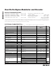
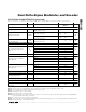
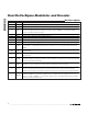
ABSOLUTE MAXIMUM RATINGS
ELECTRICAL CHARACTERISTICS
(V
DD
= 2.7V to 3.6V, T
A
= -40°C to +85°C, f
CLK
= 8MHz, V
REF
= internal, OSR = 128, unless otherwise noted.) (Note 1)
Stresses beyond those listed under “Absolute Maximum Ratings” may cause permanent damage to the device. These are stress ratings only, and functional
operation of the device at these or any other conditions beyond those indicated in the operational sections of the specifications is not implied. Exposure to
absolute maximum rating conditions for extended periods may affect device reliability.
Voltage Range on V
DD
Relative to DGND.............-0.3V to +4.0V
Voltage Range on V
DD
Relative to AGND.............-0.3V to +4.0V
Voltage Range on AGND Relative to DGND .........-0.3V to +0.3V
Voltage Range on Any Pin Relative to DGND
Except AN0+, AN0-, and AN1+, AN1- ...............-0.3V to +4.0V
Voltage Range on AN0+, AN0-, AN1+, and AN1-
Relative to AGND ...............................................-4.0V to +4.0V
Operating Temperature Range ...........................-40°C to +85°C
Storage Temperature Range .............................-65°C to +150°C
Soldering Temperature...........................Refer to the IPC/JEDEC
J-STD-020 Specification.
PARAMETER SYMBOL CONDITIONS MIN
TYP
(Note 2)
MAX UNITS
Supply Voltage V
DD
V
RST
3.3 3.6 V
Power-Fail Reset Voltage V
RST
Monitors V
DD
2.7 2.8 2.99 V
Active V
DD
Current I
DD
Normal operation 3.5 5.0 mA
Shutdown (Power-Down) V
DD
Current
I
STOP
RST = 0 or V
DD
< V
RST
2 nA
Input Low Voltage V
IL
DGND 0.3 x V
DD
V
Input High Voltage V
IH
0.7 x V
DD
V
DD
V
Output Low Voltage
(CLKIO, MNOUT)
V
OL
I
OL
= 4mA DGND 0.4 V
Output High Voltage
(CLKIO, MNOUT)
V
OH
I
OH
= -4mA V
DD
- 0.4 V
Input/Output Pin Capacitance C
IO
(Note 3) 15 pF
Input Leakage Current (All Inputs) I
L
-100 +100 nA
CLOCK SOURCE
External Clock Input Frequency f
XCLK
CLKSEL = 1 DC 8 MHz
External Clock Input Period t
XCLK-CLCL
CLKSEL = 1 125 ns
External Clock Input Duty Cycle t
XCLK-DUTY
CLKSEL = 1 40 60 %
Internal Oscillator Output
Frequency
f
ICLK
CLKSEL = 0 7.5 8.0 8.5 MHz
Internal Oscillator Output Duty
Cycle
t
ICLK-DUTY
CLKSEL = 0 47.8 49.1 49.7 %
ANALOG-TO-DIGITAL CONVERTER
AFE Warmup Delay t
WU1
f
ICLK
= 8MHz (Notes 1, 4) 1.02 ms
Reference Buffer Warmup Delay t
WU2
f
ICLK
= 8MHz (Notes 1, 5) 7.17 ms
OSR = 32 16
OSR = 64 19
OSR = 128 22
Decimator Output (Note 6)
OSR = 256 24
Bits
Integral Nonlinearity INL (Notes 1, 6) ±0.01 %FSR
Offset Error Gain = 1 (Note 6) 1.4 mV