PD - 97728A IRFTS8342PbF RDS(on) max 19 m 29 m 4.8 nC 8.2 A (@VGS = 10V) RDS(on) max (@VGS = 4.
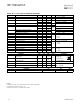
IRFTS8342PbF Static @ TJ = 25°C (unless otherwise specified) Parameter BVDSS VDSS/TJ RDS(on) Min. Typ. Max. Drain-to-Source Breakdown Voltage Breakdown Voltage Temp. Coefficient 30 ––– ––– 18 ––– ––– Static Drain-to-Source On-Resistance ––– ––– 15 22 19 29 VGS = 0V, ID = 250μA V mV/°C Reference to 25°C, ID = 1mA VGS = 10V, ID = 8.2A m VGS = 4.5V, ID = 6.6A d d VGS(th) Gate Threshold Voltage 1.35 1.80 2.35 V VGS(th) IDSS Gate Threshold Voltage Coefficient ––– -5.
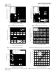
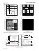
IRFTS8342PbF 100 100 VGS 10V 8.0V 7.0V 4.5V 3.5V 3.0V 2.75V 2.5V 10 BOTTOM VGS 10V 8.0V 7.0V 4.5V 3.5V 3.0V 2.75V 2.5V TOP ID, Drain-to-Source Current (A) ID, Drain-to-Source Current (A) TOP 1 2.5V 0.1 BOTTOM 10 2.5V 60μs PULSE WIDTH 60μs PULSE WIDTH Tj = 150°C Tj = 25°C 1 0.01 0.01 0.1 1 10 0.1 100 100 100 1.6 RDS(on) , Drain-to-Source On Resistance (Normalized) ID, Drain-to-Source Current (A) 10 Fig 2. Typical Output Characteristics Fig 1.
IRFTS8342PbF 1000 ID, Drain-to-Source Current (A) ISD, Reverse Drain Current (A) 100 T J = 150°C 10 T J = 25°C 1 OPERATION IN THIS AREA LIMITED BY R DS(on) 100 100μsec 1msec 10 10msec 1 0.1 Tc = 25°C Tj = 150°C Single Pulse VGS = 0V 0.1 0.01 0.2 0.4 0.6 0.8 1.0 1.2 1.4 0.01 1.6 0.1 1 10 100 VDS, Drain-toSource Voltage (V) VSD, Source-to-Drain Voltage (V) Fig 7. Typical Source-Drain Diode Forward Voltage Fig 8.
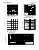
40 RDS(on), Drain-to -Source On Resistance ( m) RDS(on), Drain-to -Source On Resistance (m ) IRFTS8342PbF ID = 8.2A 35 30 25 T J = 125°C 20 15 T J = 25°C 10 0 5 10 15 90 80 70 Vgs = 4.5V 60 50 40 Vgs = 10V 30 20 10 20 0 10 20 30 40 50 60 70 80 ID, Drain Current (A) VGS, Gate -to -Source Voltage (V) Fig 13. Typical On-Resistance vs. Drain Current Fig 12. On-Resistance vs. Gate Voltage 1000 100 ID TOP 0.96A 1.5A BOTTOM 6.
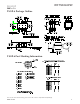
IRFTS8342PbF Id Vds Vgs L VCC DUT 0 1K Vgs(th) S Qgs1 Qgs2 Qgd Qgodr Fig 17b. Gate Charge Waveform Fig 17a. Gate Charge Test Circuit V(BR)DSS 15V DRIVER L VDS D.U.T RG + V - DD IAS 20V tp A I AS 0.01 tp Fig 18a. Unclamped Inductive Test Circuit V DS V GS RG RD VDS 90% D.U.T. + -V DD V10V GS Pulse Width µs Duty Factor Fig 19a. Switching Time Test Circuit 6 Fig 18b. Unclamped Inductive Waveforms 10% VGS td(on) tr td(off) tf Fig 19b.
IRFTS8342PbF TSOP-6 Package Outline TSOP-6 Part Marking Information < <($5 : :((. 3$57 180%(5 723 /27 &2'( 3$57 180%(5 &2'( 5()(5(1&( $ 6, '9 2 ,5/76 753%) % ,5) 3 ,5)76 753%) 5 ,5)76 753%) & ,5) 6 1RW DSSOLFDEOH ' ,5) ( ,5) 7 ,5/76 753%) ) ,5) * ,5) + ,5) , ,5) - ,5) .
IRFTS8342PbF TSOP-6 Tape & Reel Information Qualification information† Qualification level Moisture Sensitivity Level Cons umer (per JE DE C JE S D47F ††† guidelines ) MS L1 TSOP-6 ††† (per JE DE C J-S T D-020D RoHS compliant †† ) Yes Qualification standards can be found at International Rectifier’s web site http://www.irf.com/product-info/reliability Higher qualification ratings may be available should the user have such requirements.