ISD2100 DATASHEET ISD2100 Digital ChipCorder with Multi Time Programming and Digital Audio Interface -1- Publication Release Feb 9, 2010 Revision 0.
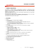
ISD2100 DATASHEET TABLE OF CONTENTS 1 GENERAL DESCRIPTION .............................................................................................................. 3 2 FEATURES ...................................................................................................................................... 3 3 BLOCK DIAGRAM ........................................................................................................................... 4 4 PINOUT CONFIGURATION ....................
ISD2100 DATASHEET 1 GENERAL DESCRIPTION The ISD2100 is a digital ChipCorder® featuring digital de-compression, comprehensive memory management, flash storage, and integrated digital audio signal paths. This family utilizes flash memory to provide non-volatile audio playback with duration up to 30 seconds (based on 8kHz/4bit ADPCM) for a single-chip solution. Unlike the MLS ChipCorder series, this device provides higher sampling frequency and a signal path with SNR equivalent to 12-bit resolution.
ISD2100 DATASHEET 3 BLOCK DIAGRAM Digital Signal Path : Digital Filters Re-sampling SPK+ PWM Control Volume Control SPK- De-Compression GPI1 / SCLK SSB GPIO2 / MISO GPIO0 / MOSI GPIO3 / INTB GPIO4 / RDY/BSYB GPIO5 SPI & GPIO Interface Memory Management and Command Interpreter Flash Memory Controller Flash Memory Figure 3-1 ISD2100 Block Diagram -4- Publication Release Feb 9, 2010 Revision 0.
ISD2100 DATASHEET SSB 3 MOSI / GPIO0 4 VSSD 5 NC NC NC NC 17 16 ISD2100 ISD2130 QFN-20 6 7 8 9 10 VCCD_PWM 2 18 SPK- SCLK / GPI1 19 VSSD_PWM 1 20 SPK+ MISO / GPIO2 NC PINOUT CONFIGURATION VCCD_PWM 4 15 GPIO5 14 VCCD 13 NC 12 RDY/BSYB / GPIO4 11 INTB / GPIO3 Figure 4-1 ISD2100 20-Lead QFN Pin Configuration. -5- Publication Release Feb 9, 2010 Revision 0.
ISD2100 DATASHEET 5 PIN DESCRIPTION Pin Number Pin Name I/O Function 1 MISO / GPIO2 O Master-In-Slave-Out. Serial output from the ISD2100 to the host. This pin is in tri-state when SSB=1. Can be configured as a general purpose I/O pin. 2 SCLK / GPI1 I Serial Clock input to the ISD2100 from the host. Can be configured as a general purpose input pin. 3 SSB I Slave Select input to the ISD2100 from the host. When SSB is low device is selected and responds to commands on the SPI interface.
ISD2100 DATASHEET SPI INTERFACE 6 This is a standard four-wire interface used for communication between ISD2100 and the host. It consists of an active low slave-select (SSB), a serial clock (SCLK), a data input (Master Out Slave In MOSI), and a data output (Master In Slave Out - MISO). In addition, for some transactions requiring data flow control, a RDY/BSYB signal (pin) is available.
ISD2100 DATASHEET TR / B SSB SCLK 0 1 2 3 4 5 6 7 0 1 2 3 4 5 6 7 RDY/BSYB =1 MISO MOSI Z =1 X PD RDY INT FULL X VG BUF BSY FUL X C7 C2 C6 C5 C4 C3 C1 CMD BSY C0 PD RDY INT FULL X VG BUF CMD BSY FUL BSY D7 D2 D6 D5 D4 D3 D1 D0 X Figure 6-2 RDY/BSYB Timing for SPI Writing Transactions. If the SCLK does not remain high, RDY bit of the status register will be set to zero and be reported via the MISO pin so the host can take the necessary actions (i.e.
ISD2100 DATASHEET TR / B SSB SCLK 0 1 2 3 4 5 6 7 0 1 2 3 4 5 6 7 RDY/BSYB =1 MISO MOSI Z =0 X PD RDY INT FULL X VG BUF CMD PD RDY INT FULL X BSY FUL BSY X C7 C2 C6 C5 C4 C3 C1 C0 D7 D6 D5 D4 D3 VG BUF CMD BSY FUL BSY D2 D1 D0 X INT Figure 6-3 SPI Transaction Ignoring RDY/BSYB -9- Publication Release Feb 9, 2010 Revision 0.
ISD2100 DATASHEET ANALOG AND DIGITAL SIGNAL PATH 7 7.1.1 PWM Speaker Driver PWM driver output pins SPK-, together with SPK+ pin, provides a differential output to drive 8Ω speaker or buzzer. During power down these pins are in tri-state. 7.1.
ISD2100 DATASHEET 8.1.3 GPIO Voice Trigger Macros: The ISD2100 GPIO flexibility allows the user to configure the device to triggers a voice macro in many different combinations for a push button application. Below is some possible configuration of the GPIO pins using Voice trigger macros? 1. Single Hi-Low trigger sequence through messages A high to low trigger on any GPIO 0~ 5 will start to play Voice Macro 3, 4, 5, 6 and back to Voice Macro 3.
ISD2100 DATASHEET 9 ELECTRICAL CHARACTERISTICS OPERATING CONDITIONS 9.1 OPERATING CONDITIONS (INDUSTRIAL PACKAGED PARTS) CONDITIONS VALUES Operating temperature range (Case temperature) Supply voltage (VDD) Ground voltage (VSS) Input voltage (VDD) -40°C to +85°C [1] +2.7V to +3.6V [2] 0V [1] 0V to 3.6V Voltage applied to any pins NOTES: 9.2 (VSS –0.3V) to (VDD +0.3V) [1] VDD = VCCA = VCCD = VCCPWM [2] VSS = VSSA = VSSD = VSSPWM AC PARAMETERS 9.2.
ISD2100 DATASHEET Output Low Voltage VOL VSS-0.3 0.3xVDD V IOL = 1mA Output High Voltage VOH 0.7xVDD VDD V IOH = -1mA INTB Output Low Voltage VOH1 0.4 V Playback Current IDD_Playback 5 Standby Current ISB 1 Input Leakage Current IIL [1] Notes: 9.3.2 mA No Load 10 µA VDD= 3.
ISD2100 DATASHEET SYMBOL TFALL DESCRIPTION Fall Time for All Digital Signals st MIN TYP MAX UNIT --- --- 10 ns TSSBS SSB Falling Edge to 1 SCLK Falling Edge Setup Time 30 --- --- ns TSSBH Last SCLK Rising Edge to SSB Rising Edge Hold Time 30ns --- 50us --- TSSBHI SSB High Time between SSB Lows 20 --- --- ns TMOS MOSI to SCLK Rising Edge Setup Time 15 --- --- ns TMOH SCLK Rising Edge to MOSI Hold Time 15 --- --- ns TZMID Delay Time from SSB Falling Edge to MISO Activ
ISD2100 DATASHEET 10 APPLICATION DIAGRAM The following applications example is for references only. It makes no representation or warranty that such applications shall be suitable for the use specified. Each design has to be optimized in its own system for the best performance on voice quality, current consumption, functionalities and etc. V CCD 14 V CCD uF 0 .01 uF 4.7 uF 0 .
ISD2100 DATASHEET 11 11.1 PACKAGE SPECIFICATION 20 LEAD QFN TOP VI EW 15 BOTTOM VI EW 11 11 10 10 16 20 16 20 6 6 1 15 5 5 - 16 - 1 Publication Release Feb 9, 2010 Revision 0.
ISD2100 DATASHEET 12 ORDERING INFORMATION I21XX X Y I R R: Tape and Reel Temperature I: Industrial -40°C to 85°C Duration 30: 30 Seconds * Based on 8kHz/4bit ADPCM Package Option Y: green Package Type Y: 20L-QFN - 17 - Publication Release Feb 9, 2010 Revision 0.
ISD2100 DATASHEET 13 REVISION HISTORY Version Date Description 0.2 Jan 29, 2009 Initial draft. 0.45 August 5, 2009 Add Wake-Up VM description 0.46 November 11, 2009 Add Checksum Description 0.48 January 9, 2010 Simplify all Block diagrams 0.51 Feb 4, 2010 Update description - 18 - Publication Release Feb 9, 2010 Revision 0.
ISD2100 DATASHEET Nuvoton products are not designed, intended, authorized or warranted for use as components in systems or equipment intended for surgical implantation, atomic energy control instruments, airplane or spaceship instruments, transportation instruments, traffic signal instruments, combustion control instruments, or for other applications intended to support or sustain life.