
User Manual
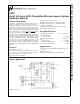
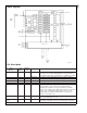
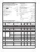
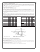

Block Diagram
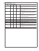
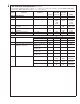
Pin Description
Pin
Name(s)
Pin
Number
Number
of Pins
Type Description
A0/NTEST_OUT 1 1 Digital I/0 The lowest order programmable bit of the serial bus address. This
pin functions as an output during NAND Tree tests (board-level
connectivity testing). Refer to
SECTION 11
on NAND Tree testing.
A1 2 1 Digital Input The highest order programmable bit of the serial bus address.
SMBData 3 1 Digital I/O Serial Bus bidirectional Data. Open-drain output.
SMBCLK 4 1 Digital Input Serial Bus Clock.
FAN1-FAN2 5-6 2 Digital Inputs Schmitt Trigger fan tachometer inputs.
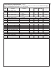
CI 7 1 Digital I/O An active high input from an external circuit which latches a
Chassis Intrusion event. This line can go high without any
clamping action regardless of the powered state of the LM81.
There is also an internal open-drain output on this line, controlled
by Bit 6 of the Configuration Register (40h) or Bit 7 CI Clear
Register (46h), to provide a minimum 20 ms reset pulse. See
Section 3.3
and
Section 9.0
.
T_CRIT_A
8 1 Digital Output Critical Temperature Alarm active low open-drain output. This pin
can be grounded when not used.
V
+
(+2.8V to
+3.8V)
9 1 POWER +3.3V V
+
power. Bypass with the parallel combination of 10 µF
(electrolytic or tantalum) and 0.1 µF (ceramic) bypass capacitors.
DS100072-2
LM81
www.national.com3