
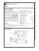
User Manual
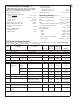

Absolute Maximum Ratings (Notes 1, 2)
If Military/Aerospace specified devices are required,
please contact the National Semiconductor Sales Office/
Distributors for availability and specifications.
Positive Supply Voltage (V
+
) +6.0V
Voltage on Any Input or Output Pin:
+12Vin, T_CRIT_A
−0.3V to +15V
A0, A1, DACOut −0.3V to (V
+
+ 0.3V)
+2.5Vin, +3.3Vin (Note 3)
All other pins −0.3V to +6V
Input Current at any Pin (Note 4)
±
5mA
Package Input Current (Note 4)
±
20 mA
Maximum Junction Temperature
(T
J
max) 150˚C
ESD Susceptibility (Note 6)
Human Body Model 2000V
Machine Model 200V
Soldering Information
MTC Package (Note 7) :
Vapor Phase (60 seconds) 215˚C
Infrared (15 seconds) 235˚C
Storage Temperature −65˚C to +150˚C
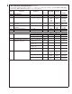
Operating Ratings (Notes 1, 2)
Operating Temperature Range T
MIN
≤ T
A
≤ T
MAX
LM81 −40˚C ≤ T
A
≤ +125˚C
Specified Temperature Range T
MIN
≤ T
A
≤ T
MAX
LM81 −40˚C ≤ T
A
≤ +125˚C
Junction to Ambient Thermal Resistance (θ
JA
(Note 5))
NS Package Number: MTC24B 95˚C/W
Supply Voltage (V
+
) +2.8V to +3.8V
V
IN
Voltage Range:
+12Vin −0.05V to +15V
+5Vin −0.05V to +6.8V
+3.3Vin −0.05V to +4.6V
+2.5Vin −0.05V to +3.6V
VID0 - VID4, Vccp, FAN1-FAN2 −0.05V to +6.0V
All other inputs −0.05V to (V
+
+ 0.05V)
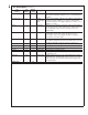
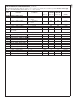
DC Electrical Characteristics
The following specifications apply for +2.8V
DC
≤ V
+
≤ +3.8V
DC
,R
S
= 500Ω, unless otherwise specified. Boldface limits apply
for T
A
=T
J
=T
MIN
to T
MAX
; all other limits T
A
=T
J
= 25˚C. (Note 8)
Symbol Parameter Conditions
Typical Limits
LM81BIM
Limits
LM81CIM
Units
(Note 9) (Note 10) (Note 10) (Limits)
POWER SUPPLY CHARACTERISTICS
I
+
Supply Current Interface Inactive 0.4 1.4 0.9 mA (max)
TEMPERATURE-TO-DIGITAL CONVERTER CHARACTERISTICS
Error −40˚C ≤ T
A
≤ +125˚C
±
3
±
3 ˚C (max)
Resolution 9-bit mode
12-bit mode
0.5
0.0625
0.5
0.0625
˚C (min)
˚C (min)
LM81 ANALOG-TO-DIGITAL CONVERTER CHARACTERISTICS
Resolution 8 bits
TUE Total
Unadjusted
Error
+2.5Vin,
+3.3Vin,
+5Vin
(Notes 11, 12) +1.2
−1.2
+2
+0.8
% (max)
% (min)
Vccp1,
Vccp2
(Note 11) +1.2
−1.2
+2.4
0
% (max)
% (min)
+12Vin (Notes 11, 12) +1.2
−1.2
+3.1
+1.2
% (max)
% (min)
DNL Differential Non-Linearity
±
1
±
1 LSB (max)
PSS Power Supply Sensitivity
±
0.4 %/V
t
C
Total Monitoring Cycle Time (Note 13)
9-bit Temp Resolution
12-bit Temp Resolution
0.4
0.82
1.2
0.82
1.2
sec
sec (max)
sec (max)
ADC INPUT CHARACTERISTICS
Input Resistance (All analog
inputs except Vccp1 and Vccp2)
115 90 90 kΩ (min)
Vccp1 and Vccp2 DC Input
Current
±
1µA
LM81
www.national.com5