
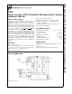
User Manual
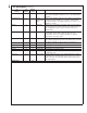
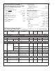

DC Electrical Characteristics (Continued)
The following specifications apply for +2.8V
DC
≤ V
+
≤ +3.8V
DC
,R
S
= 500Ω, unless otherwise specified. Boldface limits apply
for T
A
=T
J
=T
MIN
to T
MAX
; all other limits T
A
=T
J
= 25˚C. (Note 8)
Symbol Parameter Conditions
Typical Limits
LM81BIM
Limits
LM81CIM
Units
(Note 9) (Note 10) (Note 10) (Limits)
DIGITAL OUTPUTS (NTEST_OUT)
V
OUT(1)
Logical “1” Output Voltage I
OUT
=
±
3.0 mA at
V
+
= +2.8V
2.4 2.4 V (min)
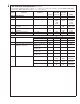
V
OUT(0)
Logical “0” Output Voltage I
OUT
=
±
3.0 mA at
V
+
= +3.8V
0.4 0.4 V (max)
OPEN- DRAIN DIGITAL OUTPUTS (SMBData, RESET, CI, INT, T_CRIT_A)
V
OUT(0)
Logical “0” Output Voltage I
OUT
= −3.0 mA 0.4 0.4 V (min)
I
OH
High Level Output Current V
OUT
=V
+
0.1 100 100 µA (max)
RESET and Chassis Intrusion
45 20 20 ms (min)
Pulse Width
DIGITAL INPUTS: VID0–VID4, NTEST_IN, A0/NTEST_OUT, A1, Chassis Intrusion (CI)
V
IN(1)
Logical “1” Input Voltage 2.0 2.0 V (min)
V
IN(0)
Logical “0” Input Voltage 0.8 0.8 V (max)
SMBus DIGITAL INPUTS (SMBCLK, SMBData)
V
IN(1)
Logical “1” Input Voltage 2.1 1.4 V (min)
V
IN(0)
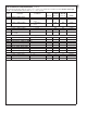
Logical “0” Input Voltage 0.8 0.6 V (max)
Tach Pulse Logic Inputs (FAN1, FAN2)
V
IN(1)
Logical “1” Input Voltage 0.7xV
+
0.7xV
+
V (min)
V
IN(0)
Logical “0” Input Voltage 0.3xV
+
0.3xV
+
V (max)
ALL DIGITAL INPUTS
I
IN(1)
Logical “1” Input Current V
IN
=V
+
−0.005 −1 −1 µA (min)
I
IN(0)
Logical “0” Input Current V
IN
=0V
DC
0.005 11µA (max)
C
IN
Digital Input Capacitance 20 pF
LM81
www.national.com7