
User Manual

AC Electrical Characteristics (Continued)
Note 1: Absolute Maximum Ratings indicate limits beyond which damage to the device may occur. Operating Ratings indicate conditions for which the device is
functional, but do not guarantee specific performance limits. For guaranteed specifications and test conditions, see the Electrical Characteristics. The guaranteed
specifications apply only for the test conditions listed. Some performance characteristics may degrade when the device is not operated under the listed test
conditions.
Note 2: All voltages are measured with respect to GND, unless otherwise specified.
Note 3: The Absolute maximum input range for :
+2.5Vin - −0.3V to (1.4 x V
+
+ 0.42V or 6V, whichever is smaller
+3.3Vin - −0.3V to (1.8 x V
+
+ 0.55V or 6V, whichever is smaller.
Note 4: When the input voltage (V
IN
) at any pin exceeds the power supplies (V
IN
<
GND or V
IN
>
V
+
), the current at that pin should be limited to 5 mA. The 20 mA
maximum package input current rating limits the number of pins that can safely exceed the power supplies with an input current of 5 mA to four.
Note 5: The maximum power dissipation must be derated at elevated temperatures and is dictated by T
J
max, θ
JA
and the ambient temperature, T
A
. The maximum
allowable power dissipation at any temperature is P
D
=(T
J
max−T
A
)/θ
JA
.
Note 6: The human body model is a 100 pF capacitor discharged through a 1.5 kΩ resistor into each pin. The machine model is a 200 pF capacitor discharged
directly into each pin.
Note 7: See the section titled “Surface Mount” found in any post 1986 National Semiconductor Linear Data Book for other methods of soldering surface mount
devices.
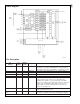
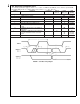
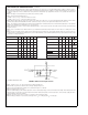
Note 8: Parasitics and or ESD protection circuitry are shown in the figure below for the LM81’s pins. The nominal breakdown voltage of the zener D3 is 6.5V. Care
should be taken not to forward bias the parasitic diode, D1, present on pins: A0/NTEST_OUT, A1 and DACOut/NTEST_IN. Doing so by more than 50 mV may corrupt
a temperature or voltage measurement.
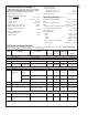
Pin Name D1 D2 D3 D4 R1 R2 Pin Name D1 D2 D3 D4 R1 R2
INT
xx 0
∞
+12Vin x x x R1+R2
∼120k
CI x x 0
∞
Vccp1, Vccp2 x x 0
∞
FAN1–FAN2 x 0
∞
+5Vin x x x R1+R2
∼120k
SMBCLK x 0
∞
+3.3Vin, +2.5Vin x x x R1+R2
∼120k
SMBData x x 0
∞
T_CRIT_A xx0
∞
RESET xx 0
∞
VID4–VID0 x x 0
∞
A0/NTEST_OUT x x x 0
∞
DACOut/NTEST_IN x x x 0
∞
A1 xxx 0
∞
Note 9: Typicals are at T
J
=T
A
= 25˚C and represent most likely parametric norm.
Note 10: Limits are guaranteed to National’s AOQL (Average Outgoing Quality Level).
Note 11: TUE (Total Unadjusted Error) includes Offset, Gain and Linearity errors of the ADC.
Note 12: Guaranteed at 3/4 scale
±
15%.
Note 13: Total Monitoring Cycle Time includes temperature conversion, 6 analog input voltage conversions and 2 tachometer readings. Each 9-bit temperature and
8-bit input voltage conversion takes 50 ms typical and 56 ms maximum. Twelve bit temperature conversion takes 400 ms. Fan tachometer readings take 20 ms
typical, at 4400 rpm, and 200 ms maximum.
Note 14: The total fan count is based on 2 pulses per revolution of the fan tachometer output.
Note 15: Timing specifications are tested at the specified logic levels, V
IL
for a falling edge and V
IH
for a rising edge.
DS100072-5
An x indicates that the diode exists.
FIGURE 2. ESD Protection Input Structure
LM81
www.national.com9