LM93 Hardware Monitor with Integrated Fan Control for Server Management 1.0 General Description The LM93, hardware monitor, has a two wire digital interface compatible with SMBus 2.0. Using an 8-bit Σ∆ ADC, the LM93 measures the temperature of two remote diode connected transistors as well as its own die and 16 power supply voltages. To set fan speed, the LM93 has two PWM outputs that are each controlled by up to four temperature zones. The fancontrol algorithm is lookup table based.
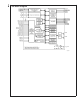
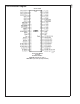
LM93 6.0 Block Diagram 20068201 www.national.
Baseboard management of a Dual processor server. Two LM93s may be required to manage a quad processor base- 2 Way Xeon Server Management 20068205 3 www.national.com LM93 board. The block diagram of LM93 hardware is illustrated below. The hardware implementation is a single chip ASIC solution. 7.
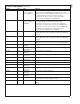
LM93 Table of Contents 1.0 General Description ..................................................................................................................................... 1 2.0 Features ....................................................................................................................................................... 1 3.0 Key Specifications ........................................................................................................................................
LM93 Table of Contents (Continued) 15.6 ERROR STATUS REGISTERS ............................................................................................................. 15.6.1 ASF Mode ........................................................................................................................................ 15.7 MASKING, ERROR STATUS AND ALERT ........................................................................................... 15.8 LAYOUT AND GROUNDING ............................
LM93 Table of Contents (Continued) 16.7.3 Registers 90–AFh Voltage Limit Registers ................................................................................... 58 16.7.4 Register B0–B1h PROCHOT User Limit Registers ...................................................................... 59 16.7.5 Register B2–B3h Dynamic Vccp Limit Offset Registers ............................................................... 60 16.7.6 Register B4–BBh Fan Tach Limit Registers .......................................
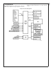
LM93 8.0 Connection Diagram 56 Pin TSSOP 20068202 NS Package MTD56 Top View NS Order Numbers: LM93CIMT (34 units per rail), or LM93CIMTX (1000 units per tape-and-reel) 7 www.national.
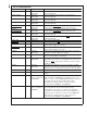
LM93 9.0 Pin Descriptions Symbol Pin # Type Function GPIO_0/TACH1 1 Digital I/O (Open-Drain) Can be configured as fan tach input or a general purpose open-drain digital I/O. GPIO_1/TACH2 2 Digital I/O (Open-Drain) Can be configured as fan tach input or a general purpose open-drain digital I/O. GPIO_2/TACH3 3 Digital I/O (Open-Drain) Can be configured as fan tach input or a general purpose open-drain digital I/O.
LM93 9.0 Pin Descriptions (Continued) Symbol Pin # Type Function REMOTE2− 21 Remote Thermal Diode_2 - Input (CPU2 THERMDC) This is the negative input (current sink) from the CPU2 thermal diode. Connected to THERMDC pin of Pentium processor or the emitter of a diode connected MMBT3904 NPN transistor. Serves as the negative input into the A/D for thermal diode voltage measurements. A 100 pF capacitor is optional and can be connected between REMOTE2− and REMOTE2+.
LM93 9.0 Pin Descriptions (Continued) Symbol Pin # Type Function AD_IN16 39 POWER (VDD) +3.3V standby power VDD power input for LM93. Generally this is connected to +3.3V standby power. The LM93 can be powered by +3.3V if monitoring in low power states is not required, but power should be applied to this input before any other pins. This pin also serves as the analog input to monitor the 3.3V stand-by (SB) voltage. It is necessary to bypass this pin with a 0.1 µF in parallel with 100 pF.
(Continued) POR Power On Reset PS Power Supply LM93 10.0 Server Terminology MTTR Mean time to repair NIC Network Interface Card (Ethernet Card) OS Operating system SMBCLK and These signals comprise the SMBus SMBDAT interface (data and clock) See the SMBus Interface section for more information. P/S Power Supply VRD PCI PCI Local Bus PDB Power Distribution Board Voltage Regulator Down - regulates Vccp voltage for a CPU 11.
LM93 The LM93 acquires temperature data from three different sources: 12.0 Functional Description The LM93 provides 16 channels of voltage monitoring, two remote thermal diode monitors, an onboard ambient temperature sensor, 2 PROCHOT monitors, 4 fan tachometers, 8 GPIOs, THERMTRIP monitor for masking error events, 2 SCSI_TERM inputs, and all the associated limit registers on a single chip, which communicates to the rest of the baseboard over the System Management Bus (SMBus).
to bring the −12V rail into the positive input voltage region of the A/D input. It is suggested that the supply rail for the LM93 device be used as the offset voltage. This voltage is usually derived from the P/S 5V stand-by voltage rail via a ± 1% accurate linear regulator. In this fashion we can always assume that the offset voltage is present when the −12V rail is present as the system cannot be turned on without the 3.3V stand-by voltage being present.
LM93 12.0 Functional Description (Continued) Required External Level Shifting Resistors for −12V Power Input 20068210 The +3.3V standby voltage is used as a reference for the level shifting. Therefore, the tolerance of this voltage directly effects the accuracy of the −12V reading. To minimize ratio errors, a tolerance of better than ± 1% should be used.
The VID signal can be changed by the processor under program control, by internal thermal events or by external control, like force PROCHOT. (Continued) Value Register VIN % ∆ from −12V 77 -11.6758 2.7014 78 -11.6511 2.9072 79 -11.6264 3.1130 80 -11.6018 3.3188 81 -11.5771 3.5245 82 -11.5524 3.7303 83 -11.5277 3.9361 84 -11.5030 4.1418 85 -11.4783 4.3476 86 -11.4536 4.5534 87 -11.4289 4.7591 88 -11.4042 4.9649 89 -11.3795 5.1707 90 -11.3548 5.3765 91 -11.
LM93 12.0 Functional Description To achieve the second goal, the LM93 has several comparators that compare the measured percentage reading against several fixed and 1 variable value. The variable value is user programmable. (Continued) mented to a max count for an above temperature trip and decremented to zero when below the trip temperature setting, to remove the trip. The minimum time for PROCHOT assertion is time dependant on the FSB frequency.
LM93 12.0 Functional Description 13.0 Inputs/Outputs (Continued) Besides all the pins associated with sensor inputs the LM93 has several pins that are assigned for other specific functions. is configured to short the PROCHOT signals together, it always asserts them together whenever this function is enabled. 13.1 ALERT OUTPUT The ALERT output is an active-low open drain output signal.
LM93 13.0 Inputs/Outputs the targeted slave address match those of the LM93 slave address. Once the address has been latched, the LM93 continues to use that address for all future transactions until power is lost. (Continued) of these issues caused problems that were difficult to work around so moving to monitoring the fuse was selected as the solution. These inputs do not have to be used for monitoring SCSI fuses.
14.5 SERIAL INTERFACE PROTOCOLS (Continued) The LM93 contains volatile registers, the registers occupy address locations from 00h to EFh. telling the slave device to expect a block write, or it may simply be a register address that tells the slave where subsequent data is to be written. Since data can flow in only one direction as defined by the R/W bit, it is not possible to send a command to a slave device during a read operation.
LM93 14.0 SMBus Interface (Continued) 14.5.
LM93 14.0 SMBus Interface (Continued) 14.5.3.3 SMBus Write Block to Any Address The start address for a block write is embedded in this transaction. In this operation the master sends a block of data to the slave as follows: 1. The master device asserts a START condition. 2. 3. The master sends the 7-bit slave address followed by the write bit (low). The addressed slave device asserts ACK. 4. The master sends a command code that tells the slave device to expect a block write.
LM93 14.0 SMBus Interface (Continued) 14.5.4 Read Operations The LM93 uses the following SMBus read protocols. 14.5.4.1 Read Byte In the LM93, the read byte protocol is used to read a single byte of data from a register. In this operation the master device receives a single byte from a slave device, as follows: 1. The master device asserts a START condition. 2. The master sends the 7-bit slave address followed by the write bit (low). 3. 4. The addressed slave device asserts ACK.
LM93 14.0 SMBus Interface (Continued) 12. The master receives byte 1 and then asserts ACK. 13. The master receives byte 2 and then asserts ACK. 14. The master receives N-3 data bytes, and asserts ACK for each one. 15. The master receives data byte N and asserts a NACK. 16. The master asserts a STOP condition to end the transaction.
LM93 14.0 SMBus Interface (Continued) 14.5.4.4 Simulated SMBus Block-Write Block-Read Process Call Alternatively, if the master cannot support an SMBus Block-Write Block-Read process call, it can be emulated by two transactions (a block write followed by a block read). This should only be done in a single master system, since in a dual master system collisions can occur that corrupt the data and transaction. Below is the sequence of events for these transactions: 1. 2.
LM93 14.0 SMBus Interface (Continued) 5. The master sends a repeated START. 6. 7. The master sends the 7-bit slave address followed by a read bit (high). The slave asserts an ACK. 8. 9. The master receives the Byte Count (depends on the Fixed Block Command Code used) and asserts an ACK. The master receives the first data byte and asserts an ACK. 10. The master continues to receive data bytes and asserting an ACK. 11. The master receives the last data byte. 12. The master asserts a NACK. 13.
LM93 14.0 SMBus Interface (Continued) Register Types Whenever the low byte of a 16-bit register is written, the write is buffered and does not take effect until the corresponding high byte is written. If the low byte of a different 16-bit register is written, the previously buffered low byte of the first register is discarded. If a device attempts to write the high byte of a 16-bit register, and the corresponding low byte was not written (or was discarded), then the LM93 will NACK the byte.
Channel # Input 15.7 MASKING, ERROR STATUS AND ALERT Masking is always applied to bits in the HOST and BMC Error Status registers. If an event is masked, the corresponding error bit in the HOST or BMC Error Status registers is prevented from ever being set. As a result, this prevents the event from ever causing ALERT to be asserted. Masking an event does not clear its associated Error Status bit if it is currently set.
LM93 15.0 Using The LM93 15.9.2 PCB Layout for Minimizing Noise In the following guidelines, D+ and D− refer to the REMOTE1+, REMOTE1−, REMOTE2+, REMOTE2− pins. (Continued) Thermal Diode Temperature vs. LM93 Temperature Reading In a noisy environment, such as a power supply, layout considerations are very critical. Noise induced on traces running between the remote temperature diode sensor and the LM93 can cause temperature conversion errors. The following guidelines should be followed: 1. Place a 0.
offset value of 4 bits. This offset gets added in a cumulative manner to the 8-bit base temperature. The calculated temperature is then used in the comparison that determines the PWM output duty cycle. The minimum PWM (minPWM) value sets the duty cycle when the measured temperature is less than or equal to the base temperature.
LM93 15.0 Using The LM93 (Continued) Zone 1/2 (CPU1 and CPU2) Table In this example: Zones 1 and 2 are bound to the PWM1 output and the PWM1 frequency set to a value in the low range; Hysteresis is set to 2˚C; Toffset and hysteresis resolution is set to 0.5˚C; minPWM register set to 05h for Zones 1/2. Note, the duty cycle assignment depends on the zone to PWM output binding and the frequency setting of that PWM output.
The low frequency PWM output duty cycle mapping is listed in the following table: (Continued) Note that since zones 1 and 2 share the same lookup table, both zones must be operating in the same resolution mode. The same applies to zones 3 and 4 since they share the same lookup table. 4-Bit Value Step Low Frequencies Duty Cycle 0h 15.10.3 Zone 1-4 to PWM1-2 Binding Each zone must be bound to the PWM outputs in order to have effect on the output’s duty cycle.
LM93 15.0 Using The LM93 PWM1/VRD2 PWM2/VRD1 PWM2/VRD2 (Continued) 15.10.8 VRDx_HOT Ramp-Up/Ramp-Down This function causes the duty cycle of the PWM outputs to gradually increase over time if VRD1_HOT or VRD2_HOT are asserted. If a PWM is bound to both VRD1_HOT and VRD2_HOT, then two ramp functions are active for that PWM output. In this case the duty cycle that is used is the maximum of the two ramp functions. When VRDx_HOT is asserted, the ramp function is enabled.
LM93 15.0 Using The LM93 (Continued) 15.11 XOR TREE TEST An XOR tree is provided in the LM93 for Automated Test Equipment (ATE) board level connectivity testing. This allows the functionality of all digital inputs to be tested in a simple manner and any pins that are non-functional or shorted together to be identified. When the test mode is enabled by setting the ‘XEN’ bit in the XOR Test register, the part enters XOR test mode.
LM93 16.0 Registers 16.1 REGISTER WARNINGS In most cases, reserved registers and register bits return zero when read. This should not be relied upon, since reserved registers can be used for future expansion of the LM93 functions. Some registers have “N/D” for their default value. This means that the power-up default of the register is not defined.
Lock LM93 16.
LM93 16.
Lock LM93 16.
LM93 16.
Lock LM93 16.
LM93 16.0 Registers (Continued) 16.3 FACTORY REGISTERS 00h–3Fh 16.3.1 Register 00h XOR Test Register Address Read/ Write Register Name 00h R/W XOR Test Bit 7 Bit 6 Bit 5 Bit 4 Bit 3 Bit 2 Bit 1 RES Bit 0 Default Value XEN 00h Sleep Masking Bit Name R/W Default Description 0 XEN R/W 0 The LM93 incorporates an XOR tree test mode. When the test mode is enabled by setting this bit, the part enters XOR test mode. Clearing this bit brings the part out of XOR test mode.
LM93 16.0 Registers (Continued) 16.4 BMC ERROR STATUS REGISTERS 40h–47h The B_Error Status Registers contain several bits that each represent a particular error event that the LM93 can monitor. The LM93 sets a given bit whenever the corresponding error event occurs. The BMC_ERR bit in the LM93 Status/Control register is also set if any bit in the BMC Error Status registers is set. If enabled, ALERT is also asserted anytime BMC_ERR is set.
LM93 16.0 Registers 16.4.
16.4.4 Register 43h LM93 16.0 Registers (Continued) B_Error Status 4 Register Address Read/ Write Register Name Bit 7 Bit 6 Bit 5 Bit 4 Bit 3 Bit 2 43h RWC B_Error Status 4 D2_ ERR D1_ ERR DVDDP2 _ERR DVDDP1 _ERR SCSI2 _ERR SCSI1 _ERR Bit 1:0 Name RES R/W R Bit 1 Bit 0 RES Default Value 00h Sleep Masking Description Reserved N/A 2 SCSI1_ERR RWC SCSI Fuse Error This bit is set if SCSI_TERM1 has been asserted.
LM93 16.0 Registers 16.4.6 Register 45h (Continued) B_P2_PROCHOT Error Status Register Address Read/ Write Register Name Bit 7 Bit 6 Bit 5 Bit 4 Bit 3 Bit 2 Bit 1 Bit 0 Default Value 45h RWC B_P2_PROCHOT Error Status PH2 _ERR TMAX T100 T75 T50 T25 T12 T0 00h Bit Name R/W Sleep Masking Description 0 T0 RWC Set when P2_PROCHOT has had a throttled event. This bit is set for any amount of PROCHOT throttling > 0%.
16.4.8 Register 47h (Continued) B_Fan Error Status Register Address Read/ Write Register Name 47h RWC B_Fan Error Status Bit Name LM93 16.0 Registers Bit 7 Bit 6 Bit 5 Bit 4 RES R/W Bit 3 Bit 2 Bit 1 Bit 0 Default Value FAN4 _ERR FAN3 _ERR FAN2 _ERR FAN1 _ERR 00h Sleep Masking Description 0 FAN1_ERR RWC This bit is set when the Fan Tach 1 value register is above the value set in the Fan Tach 1 Limit register.
LM93 16.0 Registers 16.5.
16.5.3 Register 4Ah LM93 16.
LM93 16.0 Registers 16.5.4 Register 4Bh (Continued) H_Error Status 4 Register Address Read/ Write Register Name Bit 7 Bit 6 Bit 5 Bit 4 Bit 3 Bit 2 4Bh RWC H_Error Status 4 D2_ ERR D1_ ERR DVDDP2 _ERR DVDDP1 _ERR SCSI2 _ERR SCSI1 _ERR Bit 1:0 Name RES R/W R Bit 1 Bit 0 RES Description Reserved Default Value 00h Sleep Masking N/A 2 SCSI1_ERR RWC SCSI Fuse Error This bit is set if SCSI_TERM1 has been asserted.
16.5.5 Register 4Ch LM93 16.0 Registers (Continued) H_P1_PROCHOT Error Status Register Address Read/ Write Register Name Bit 7 Bit 6 Bit 5 Bit 4 Bit 3 Bit 2 Bit 1 Bit 0 Default Value 4Ch RWC H_P1_PROCHOT Error Status PH1_ERR TMAX T100 T75 T50 T25 T12 T0 00h Bit Name R/W Description Sleep Masking 0 T0 RWC Set when P1_PROCHOT has had a throttled event. This bit is set for any amount of PROCHOT throttling > 0%.
LM93 16.0 Registers 16.5.6 Register 4Dh (Continued) B_P2_PROCHOT Error Status Register Address Read/ Write Register Name Bit 7 Bit 6 Bit 5 Bit 4 Bit 3 Bit 2 Bit 1 Bit 0 Default Value 4Dh RWC H_P2_PROCHOT Error Status PH2_ERR TMAX T100 T75 T50 T25 T12 T0 00h Bit Name R/W Description Sleep Masking 0 T0 RWC Set when P2_PROCHOT has had a throttled event. This bit is set for any amount of PROCHOT throttling > 0%.
16.5.7 Register 4Eh LM93 16.0 Registers (Continued) H_GPI Error Status Register Address Read/ Write Register Name Bit 7 Bit 6 Bit 5 Bit 4 Bit 3 Bit 2 Bit 1 Bit 0 Default Value 4Eh RWC H_GPI Error Status GPI7 _ERR GPI6 _ERR GPI5 _ERR GPI4 _ERR GPI3 _ERR GPI2 _ERR GPI1 _ERR GPI0 _ERR 00h Bit Name R/W Description Sleep Masking 0 GPI0_ERR RWC This bit is set whenever GPIO0 is driven low (unless masked via the GPI Error Mask register).
LM93 16.0 Registers 16.5.8 Register 4Fh (Continued) H_Fan Error Status Register Address Read/ Write Register Name 4Fh RWC H_Fan Error Status Bit Name Bit 7 Bit 6 Bit 5 Bit 4 RES R/W Bit 3 Bit 2 Bit 1 Bit 0 Default Value FAN4 _ERR FAN3 _ERR FAN2 _ERR FAN1 _ERR 00h Sleep Masking Description 0 FAN1_ERR RWC This bit is set when the Fan Tach 1 value register is above the value set in the Fan Tach 1 Limit register.
LM93 16.0 Registers (Continued) 16.6.
LM93 16.0 Registers 16.6.5 Register 68h (Continued) Average P1_PROCHOT Register Address Read/ Write Register Name Bit 7 Bit 6 Bit 5 Bit 4 Bit 3 Bit 2 Bit 1 Bit 0 Default Value 68h R Average P1_PROCHOT 7 6 5 4 3 2 1 0 N/D This is the average percentage active time of P1_PROCHOT. It is the result of adding the contents of this register to the contents of the Current P1_PROCHOT register and dividing the result by 2.
16.6.8 Register 6Bh LM93 16.0 Registers (Continued) GPI State Register Address Read/ Write Register Name Bit 7 Bit 6 Bit 5 Bit 4 Bit 3 Bit 2 Bit 1 Bit 0 Default Value 6Bh R GPI State GPI7 GPI6 GP15 GPI4 GPI3 GPI2 GPI1 GPI0 N/D Bit 2 Bit 1 Bit 0 Default Value 16.6.
LM93 16.0 Registers 16.6.
LM93 16.0 Registers (Continued) 16.7 LIMIT REGISTERS 16.7.
LM93 16.0 Registers 16.7.
16.7.4 Register B0–B1h LM93 16.0 Registers (Continued) PROCHOT User Limit Registers Register Address Read/ Write Register Name Bit 7 Bit 6 Bit 5 Bit 4 Bit 3 Bit 2 Bit 1 Bit 0 Default Value B0h R/W P1_PROCHOT User Limit 7 6 5 4 3 2 1 0 FFh B1h R/W P2_PROCHOT User Limit 7 6 5 4 3 2 1 0 FFh These registers allow a user limit to be set for the PROCHOT monitoring function.
LM93 16.0 Registers 16.7.5 Register B2–B3h (Continued) Dynamic Vccp Limit Offset Registers Register Address Read/ Write Register Name B2h R/W Vccp1 Limit Offsets UPPER_OFFSET1 LOWER_OFFSET1 17h B3h R/W Vccp2 Limit Offsets UPPER_OFFSET2 LOWER_OFFSET2 17h Bit 7 Bit 6 Bit 5 Bit 4 Bit 3 Bit 2 Bit 1 Bit 0 Default Value These offsets are used to determine the upper and lower limits of the dynamic Vccp window comparator.
LM93 16.0 Registers (Continued) 16.7.
LM93 16.0 Registers (Continued) 16.8 SETUP REGISTERS 16.8.1 Register BCh Special Function Control 1 (Voltage Hysteresis and Fan Control Filter Enable) Register Address Read/ Write Register Name Bit 7 Bit 6 Bit 5 Bit 4 Bit 3 BCh R/W Special Function Control 1 RES FCFE2 FCFE1 LCFE2 LCFE1 Bit 2 Bit 1 Bit 0 Default Value VH 00h Bit Name R/W 2:0 VH R/W Voltage hysteresis control. This determines the amount of hysteresis to be applied to all voltage limit comparisons.
16.8.2 Register BDh Control) LM93 16.
LM93 16.0 Registers 16.8.4 Register BFh (Continued) PWM Ramp Control Register Address Read/ Write Register Name BFh R/W PWM Ramp Control Bit 7 Bit 6 Bit 5 Bit 4 Bit 3 PH_RAMP Bit 2 Bit 1 Bit 0 VRD_RAMP Bit Name R/W 3:0 VRD_RAMP R/W Sets the time delay between ramp steps for the VRDx_HOT ramp up/ramp down PWM function. 7:4 PH_RAMP R/W Sets the time delay between ramp steps for the Px_PROCHOT ramp up/ramp down PWM function.
16.8.6 Register C1h LM93 16.
LM93 16.0 Registers 16.8.8 Register C3h (Continued) Zones 1/2 MinPWM and Hysteresis Register Address Read/ Write Register Name C3h R/W Zones 1/2 MinPWM and Hysteresis Bit 6 Bit 5 Bit 4 Bit 3 MinPWM Bit 2 Bit 1 Bit 0 FC_TH Bit Name R/W Description 3:0 FC_TH R/W This field sets the amount of hysteresis (in degrees C) that is used by the auto-fan control for zones 1 and 2. This should be set greater than 0 to avoid unwanted oscillation between two steps in the look-up table.
16.8.10 Register C5h LM93 16.0 Registers (Continued) GPO Register Address Read/ Write Register Name Bit 7 Bit 6 Bit 5 Bit 4 Bit 3 Bit 2 Bit 1 Bit 0 Default Value C5h R/W GPO GPO7 GPO6 GPO5 GPO4 GPO3 GPO2 GPO1 GPO0 00h Bit Name R/W Description 0 GPO0 R/W If set, GPIO_0 will be pulled low. If cleared, the output is not pulled low. This bit should be 0 if GPIO_0 is being used as an input. 1 GPO1 R/W If set, GPIO_1 will be pulled low.
LM93 16.0 Registers (Continued) 16.8.11 Register C6h PROCHOT Override Register Address Read/ Write Register Name Bit 7 Bit 6 C6h R/W PROCHOT Override FORCE _P1 FORCE _P2 Bit 5 Bit 4 Bit 3 RES Bit 2 Bit 1 PHT_DC Bit Name R/W 3:0 PHT_DC R/W 5:4 RES R 6 FORCE_P1 R/W When this is set by software, P1_PROCHOT will be asserted by the LM93 with the duty cycle selected by PHT_DC.
16.8.12 Register C7h LM93 16.0 Registers (Continued) PROCHOT Time Interval Register Address Read/ Write Register Name C7h R/W PROCHOT Time Interval Bit 7 Bit 6 Bit 5 Bit 4 Bit 3 Bit 2 P2_TI Bit 1 P1_TI Bit Name R/W 3:0 P1_TI R/W Sets the monitoring interval for P1_PROCHOT 7:4 P2_TI R/W Sets the monitoring interval for P2_PROCHOT Bit 0 Default Value 11h Description Possible settings for P1_TI and P2_TI: P1_TI or P2_TI Monitoring Time Interval (seconds) 0h 0.73 1h 1.
LM93 16.0 Registers (Continued) 16.8.13 Register C8h PWM1 Control 1 Register Address Read/ Write Register Name Bit 7 Bit 6 Bit 5 Bit 4 Bit 3 Bit 2 Bit 1 Bit 0 Default Value C8h R/W PWM1 Control 1 VRD2 VRD1 PH2 PH1 ZN4 ZN3 ZN2 ZN1 0Fh Bit Name R/W 0 ZN1 R/W If set, PWM1 will be bound to temperature zone 1. Description 1 ZN2 R/W If set, PWM1 will be bound to temperature zone 2. 2 ZNE R/W If set, PWM1 will be bound to temperature zone 3.
LM93 16.0 Registers (Continued) 16.8.14 Register C9h PWM1 Control 2 Register Address Read/ Write Register Name C9h R/W PWM1 Control 2 Bit 7 Bit 6 Bit 5 OVR_DC Bit 4 Bit 3 Bit 2 Bit 1 Bit 0 Default Value PL EPPL INV OVR 00h Bit Name R/W 0 OVR R/W When set, enables manual duty cycle override for PWM1. Description 1 INV R/W Invert PWM1 output. When 0, 100% duty cycle corresponds to the PWM output continuously HIGH.
LM93 16.0 Registers (Continued) 16.8.15 Register CAh PWM1 Control 3 Register Address Read/ Write Register Name CAh R/W PWM1 Control 3 Bit 7 Bit 6 Bit 5 Bit 4 SU_DUR Bit Name R/W 3:0 SU_DC R/W 4 RES R 7:5 SU_DUR R/W Bit 3 Bit 2 RES Bit 1 Bit 0 SU_DC Default Value 00h Description This field sets the duty cycle that will be used whenever PWM1 experiences a Spin-Up cycle.
LM93 16.0 Registers (Continued) 16.8.17 Register CCh PWM2 Control 1 Register Address Read/ Write Register Name Bit 7 Bit 6 Bit 5 Bit 4 Bit 3 Bit 2 Bit 1 Bit 0 Default Value CCh R/W PWM2 Control 1 VRD2 VRD1 PH2 PH1 ZN4 ZN3 ZN2 ZN1 0Fh Bit Name R/W 0 ZN1 R/W If set, PWM2 will be bound to temperature zone 1. Description 1 ZN2 R/W If set, PWM2 will be bound to temperature zone 2. 2 ZN3 R/W If set, PWM2 will be bound to temperature zone 3.
LM93 16.0 Registers (Continued) 16.8.18 Register CDh PWM2 Control 2 Register Address Read/ Write Register Name CDh R/W PWM2 Control 2 www.national.com Bit 7 Bit 6 Bit 5 OVR_DC Bit 4 Bit 3 Bit 2 Bit 1 Bit 0 Default Value PL EPPL INV OVR 00h Bit Name R/W 0 OVR R/W When set, enables manual duty cycle override for PWM2. Description 1 INV R/W Invert PWM1 output. When 0, 100% duty cycle corresponds to the PWM output continuously HIGH.
LM93 16.0 Registers (Continued) 16.8.19 Register CEh PWM2 Control 3 Register Address Read/ Write Register Name CEh R/W PWM2 Control 3 Bit 7 Bit 6 Bit 5 SU_DUR Bit Name R/W 3:0 SU_DC R/W 4 RES R 7:5 SU_DUR R/W Bit 4 Bit 3 Bit 2 RES Bit 1 Bit 0 SU_DC Default Value 00h Description This field sets the duty cycle that used whenever PWM2 experiences a Spin-Up cycle.
LM93 16.0 Registers (Continued) 16.8.
16.8.23 Register E0h LM93 16.0 Registers (Continued) Special Function TACH to PWM Binding Register Address Read/ Write Register Name Bit 7 Bit 6 Bit 5 Bit 4 Bit 3 Bit 2 Bit 1 Bit 0 Default Value E0h R/W Special Function TACH to PWM Binding T4P2 T4P1 T3P2 T3P1 T2P2 T2P1 T1P2 T1P1 00h Bit Name R/W Description 0 T1P1 R/W If set, TACH1 is bound to PWM1. 1 T1P2 R/W If set, TACH1 is bound to PWM2. 2 T2P1 R/W If set, TACH2 is bound to PWM1.
LM93 16.0 Registers 16.8.24 Register E2h Register Read/ Address Write E2h R/W (Continued) LM93 Status Control Register Name Bit 7 Bit 6 Bit 5 LM93 Status/ Control BMC _ERR HOST _ERR TACH_EDGE Lock X Bit 3 Bit 2 GPI5_AM GPI4_AM Bit 1 Bit 0 Default Value ASF OVRID 00h Bit Name R/W 0 OVRID R/W If this bit is set, all PWM outputs go to 100% duty cycle. 1 ASF R/W If this bit is set, BMC error registers support ASF, i.e. reset on read.
16.8.25 Register E3h LM93 16.0 Registers (Continued) LM93 Configuration Register Address Read/ Write Register Name Bit 7 E3h R/W LM93 Configuration READY Bit 6 Bit 4 Bit 3 Bit 2 Bit 1 Bit 0 Default Value P1P2_ PROCHOT ALERT _EN GMSK LOCK START 00h Bit 5 RES Lock Bit Name R/W Description x 0 START R/W When this bit is 0, the LM93 operates in basic mode. All error events are masked. The auto fan control algorithm is disabled.
LM93 16.0 Registers (Continued) 16.9 SLEEP STATE CONTROL AND MASK REGISTERS 16.9.1 Register E4h Sleep State Control Register Address Read/ Write Register Name E4h R Sleep State Control Bit 7 Bit 6 Bit 5 Bit 3 Bit 2 RES Bit Name R/W 1:0 SB R/W 7:2 RES R Bit 1 Bit 0 SB Description Sleep State Control. Setting this field tells the LM93 which sleep state the system is in. Several error events are masked depending on the state of this field. Reserved SB www.national.
16.9.2 Register E5h LM93 16.0 Registers (Continued) S1 GPI Mask Register Address Read/ Write Register Name Bit 7 Bit 6 Bit 5 Bit 4 Bit 3 Bit 2 Bit 1 Bit 0 Default Value E5h R/W S1 GPI Mask GPI7_S1 _MSK GPI6_S1 _MSK GPI5_S1 _MSK GPI4_S1 _MSK GPI3_S1 _MSK GPI2_S1 _MSK GPI1_S1 _MSK GPI0_S1 _MSK FFh Bit Name R/W 0 GPI0_S1_MSK R/W If set, GPI0 errors are masked in S1 sleep state. 1 GPI1_S1_MSK R/W If set, GPI1 errors are masked in S1 sleep state.
LM93 16.0 Registers 16.9.4 Register E7h (Continued) S3 GPI Mask Register Address Read/ Write Register Name Bit 7 Bit 6 Bit 5 Bit 4 Bit 3 Bit 2 Bit 1 Bit 0 Default Value E7h R/W S3 GPI Mask GPI7_S3 _MSK GPI6_S3 _MSK GPI5_S3 _MSK GPI4_S3 _MSK GPI3_S3 _MSK GPI2_S3 _MSK GPI1_S3 _MSK GPI0_S3 _MSK FFh Bit Name R/W 0 GPI0_S3_MSK R/W If set, GPI0 errors are masked in S3 sleep state. 1 GPI1_S3_MSK R/W If set, GPI1 errors are masked in S3 sleep state.
16.9.7 Register EAh LM93 16.0 Registers (Continued) S4/5 GPI Mask Register Address Read/ Write Register Name Bit 7 Bit 6 Bit 5 Bit 4 Bit 3 Bit 2 Bit 1 Bit 0 Default Value EAh R/W S4/5 GPI Mask GPI7 _S4/5 _MSK GPI6 _S4/5 _MSK GPI5 _S4/5 _MSK GPI4 _S4/5 _MSK GPI3 _S4/5 _MSK GPI2 _S4/5 _MSK GPI1 _S4/5 _MSK GPI0 _S4/5 _MSK FFh Bit Name R/W 0 GPI0_S4/5_MSK R/W If set, GPI0 errors are masked in S4/5 sleep state.
LM93 16.0 Registers (Continued) 16.10 OTHER MASK REGISTERS 16.10.1 Register ECh GPI Error Mask Register Address Read/ Write Register Name Bit 7 Bit 6 Bit 5 Bit 4 Bit 3 Bit 2 Bit 1 Bit 0 Default Value ECh R/W GPI Error Mask GPI7 _MSK GPI6 _MSK GPI5 _MSK GPI4 _MSK GPI3 _MSK GPI2 _MSK GPI1 _MSK GPI0 _MSK FFh Bit Name R/W 0 GPI0_MSK R/W When this bit is set, GPI0 error events are masked. Description 1 GPI1_MSK R/W When this bit is set, GPI1 error events are masked.
16.10.3 Register EEh LM93 16.0 Registers (Continued) Special Function Zone 1 Adjustment Offset Register Address Read/ Write Register Name Bit 7 Bit 6 EEh R/W Special Function Zone 1 Adjustment Offset RES RES Bit 5 Bit 4 Bit 3 Bit 2 Bit 1 Z1_ADJUST Default Value 00h Bit Name R/W Description 5:0 Z1_ADJUST R/W 6-bit signed 2’s complement offset adjustment. This value is added to all zone 1 temperature measurements as they are made.
LM93 17.0 Absolute Maximum Ratings (Notes 1, 2) ESD Susceptibility (Note 4) If Military/Aerospace specified devices are required, please contact the National Semiconductor Sales Office/ Distributors for availability and specifications. Positive Supply Voltage (VDD) 0˚C ≤ TA ≤ +85˚C Operating Temperature Range Nominal Supply Voltage −0.3V to (VDD + 0.05V) Voltage at Other Analog Voltage Inputs −65˚C to +150˚C 18.0 Operating Ratings (Notes 1, 2) −0.3V to +6.
(Continued) The following limits apply for +3.0 VDC to +3.6 VDC, unless otherwise noted. Bold face limits apply for TA = TJ over TMIN to TMAX of the operating range; all other limits TA = TJ = 25˚C unless otherwire noted. TA is the ambient temperature of the LM93; TJ is the junction temperature of the LM93; TD is the junction temperature of the thermal diode.
LM93 AC Electrical Characteristics The following limits apply for +3.0 VDC to +3.6 VDC, unless otherwise noted. Bold face limits apply for TA = TJ = TMIN to TMAX of the operating range; all other limits TA = TJ = 25˚C unless otherwire noted. Symbol Parameter Conditions Typical (Note 9) Limits (Note 10) Units (Limits) FAN RPM-TO-DIGITAL CHARACTERISTICS Counter Resolution 14 bits Number of fan tach pulses count is based on 2 pulses Counter Frequency 22.
LM93 20068203 Note 1: Absolute Maximum Ratings indicate limits beyond which damage to the device may occur. Operating Ratings indicate conditions for which the device is functional, but do not guarantee specific performance limits. For guaranteed specifications and test conditions, see the Electrical Characteristics. The guaranteed specifications apply only for the test conditions listed. Some performance characteristics may degrade when the device is not operated under the listed test conditions.
LM93 Symbol Pin # D1 D2 D4 D5 D6 SNP R1 AD_IN1 23 U U U U U AD_IN2 24 U U U U U AD_IN3 25 U U U U U AD_IN4 26 U U U U U AD_IN5 27 U U U U U AD_IN6 28 U U U U U AD_IN7 29 U U U U U AD_IN8 30 U U U U U AD_IN9 31 U U U U U AD_IN10 32 U U U U U AD_IN11 33 U U U U U AD_IN12 34 U U U U U AD_IN13 35 U U U U U AD_IN14 36 U U U U U AD_IN15 37 U U U U U ADDR_SEL 38 U AD_IN16/VDD (V+) 39 U GND 40
19.0 Data Sheet Version History Version Date 2.0 April 12, 2004 Change 1. Updated Section 16.7.2 Registers 80–83h Fan Boost Temperature Registers, changed "If set to 80h, the feature is disabled." to "If set to 7Fh and the fan control temperature resolution is 1˚C, the feature is disabled." 2. Updated Table DC Electrical Characteristics, Thermal Diode Source Current typical specifications, changed: "170" to 188" and "10.625" to "11.75". 3.
LM93 Hardware Monitor with Integrated Fan Control for Server Management 20.