
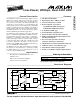
User Manual


_______________General Description
The MAX1003 is a dual, 6-bit analog-to-digital converter
(ADC) that combines high-speed, low-power operation
with a user-selectable input range, an internal refer-
ence, and a clock oscillator. The dual parallel ADCs are
designed to convert in-phase (I) and quadrature (Q)
analog signals into two 6-bit, offset-binary-coded digital
outputs at sampling rates up to 90Msps. The ability to
directly interface with baseband I and Q signals makes
the MAX1003 ideal for use in direct-broadcast satellite,
VSAT, and QAM16 demodulation applications.
The MAX1003 input amplifiers feature true differential
inputs, a -0.5dB analog bandwidth of 55MHz, and user-
programmable input full-scale ranges of 125mVp-p,
250mVp-p, or 500mVp-p. With an AC-coupled input
signal, matching performance between input channels
is typically better than 0.1dB gain, 1/4LSB offset, and
0.5° phase. Dynamic performance is 5.85 effective
number of bits (ENOB) with a 20MHz analog input sig-
nal, or 5.7 ENOB with a 50MHz signal.
The MAX1003 operates with +5V analog and +3.3V digi-
tal supplies for easy interfacing to +3.3V-logic-compati-
ble digital signal processors and microprocessors. It
comes in a 36-pin SSOP package.
________________________Applications
Direct Broadcast Satellite (DBS) Receivers
VSAT Receivers
Wide Local Area Networks (WLANs)
Cable Television Set-Top Boxes
____________________________Features
♦ Two Matched 6-Bit ADCs
♦ High Sampling Rate: 90Msps per ADC
♦ Low Power Dissipation: 350mW
♦ Excellent Dynamic Performance:
5.85 ENOB with 20MHz Analog Input
5.7 ENOB with 50MHz Analog Input
♦ ±1/4LSB INL and DNL (typ)
♦ Internal Bandgap Voltage Reference
♦ Internal Oscillator with Overdrive Capability
♦ 55MHz (-0.5dB) Bandwidth Input Amplifiers with
True Differential Inputs
♦ User-Selectable Input Full-Scale Range
(125mVp-p, 250mVp-p, or 500mVp-p)
♦ 1/4LSB Channel-to-Channel Offset Matching (typ)
♦ 0.1dB Gain and 0.5° Phase Matching (typ)
♦ Single-Ended or Differential Input Drive
♦ Flexible, 3.3V, CMOS-Compatible Digital Outputs
MAX1003
Low-Power, 90Msps, Dual 6-Bit ADC
________________________________________________________________
Maxim Integrated Products
1
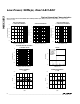
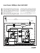
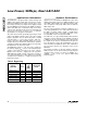
MAX1003
DATA
BUFFER
Q
CLOCK
DRIVER
DI0–DI5
DCLK
TNK+
TNK-
DQ0–DQ5
INPUT
AMP
I
IIN+
IIN-
GAIN
QIN+
QIN-
CLOCK
OUT
DATA
BUFFER
I
6
ADC
I
ADC
Q
VREF
VREF
BANDGAP
REFERENCE
OFFSET
CORREC-
TION Q
OFFSET
CORREC-
TION I
INPUT
AMP
Q
QOCC+ QOCC-
IOCC+ IOCC-
6
6
6
_________________________________________________________Functional Diagram
19-1236; Rev 0; 6/97
PART
MAX1003CAX 0°C to +70°C
TEMP. RANGE PIN-PACKAGE
36 SSOP
EVALUATION KIT
AVAILABLE
______________Ordering Information
Pin Configuration appears at end of data sheet.
For free samples & the latest literature: http://www.maxim-ic.com, or phone 1-800-998-8800