
User Manual
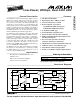


MAX1003
Low-Power, 90Msps, Dual 6-Bit ADC
2 _______________________________________________________________________________________
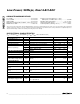
ABSOLUTE MAXIMUM RATINGS
DC ELECTRICAL CHARACTERISTICS
(V
CC
= +5V ±5%, V
CCO
= 3.3V ±300mV, T
A
= T
MIN
to T
MAX
, unless otherwise noted.)
Stresses beyond those listed under “Absolute Maximum Ratings” may cause permanent damage to the device. These are stress ratings only, and functional
operation of the device at these or any other conditions beyond those indicated in the operational sections of the specifications is not implied. Exposure to
absolute maximum rating conditions for extended periods may affect device reliability.
V
CC
to GND ............................................................-0.3V to 6.5V
V
CCO
to OGND........................................................-0.3V to 6.5V
GND to OGND ........................................................-0.3V to 0.3V
Digital and Clock Output Pins to OGND...-0.3V to V
CCO
(10sec)
All Other Pins to GND...............................................-0.3V to V
CC
Continuous Power Dissipation (T
A
= +70°C)
SSOP (derate 11.8mW/°C above +70°C) ...................941mW
Operating Temperature Range...............................0°C to +70°C
Storage Temperature Range.............................-65°C to +150°C
Lead Temperature (soldering, <10sec)...........................+300°C
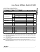
CONDITIONS
LSB-0.5 ±0.25 0.5INLIntegral Nonlinearity
Bits6RESResolution
UNITSMIN TYP MAXSYMBOLPARAMETER
GAIN = open (mid gain)
GAIN = V
CC
(high gain)
No missing codes over temperature
237.5 250 262.5V
FSM
118.75 125 131.25V
FSH
LSB-0.5 ±0.25 0.5DNLDifferential Nonlinearity
Other analog input driven with external source
(Note 2)
Guaranteed by design
V1.75 2.75V
CM
GAIN = GND (low gain)
Common-Mode Voltage Range
pF3 5C
IN
Input Capacitance
kΩ13 20 29R
IN
Input Resistance
V2.25 2.35 2.45V
AOC
Input Open-Circuit Voltage
mVp-p
475 500 525V
FSL
Full-Scale Input Range
Other oscillator input tied to V
CC
+ 0.3V
I
SOURCE
= 50µA V0.7V
CCO
V
OH
Digital Outputs Logic-High
Voltage
kΩ4.8 8 12.1R
OSC
Oscillator Input Resistance
I
SINK
= 400µA V0.5V
OL
Digital Outputs Logic-Low
Voltage
V
CC
= 4.75V to 5.25V (Note 3)
20MHz, full-scale I and Q analog inputs,
C
L
= 15pF (Note 4)
mW350PDPower Dissipation
mA21I
CCO
Digital Outputs Supply Current
dB-75 -40PSRRPower-Supply Rejection Ratio
mA63 104I
CC
Supply Current
DC ACCURACY (Note 1)
INVERTING AND NONINVERTING ANALOG INPUTS
OSCILLATOR INPUTS
DIGITAL OUTPUTS (DI0–DI5, DQ0–DQ5)
POWER SUPPLY