
User Manual
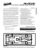


MAX1003
Low-Power, 90Msps, Dual 6-Bit ADC
_______________________________________________________________________________________ 3
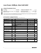
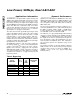
AC ELECTRICAL CHARACTERISTICS
(V
CC
= +5V ±5%, V
CCO
= 3.3V ±300mV, T
A
= +25°C, unless otherwise noted.)
Note 1: Best-fit straight-line linearity method.
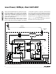
Note 2: A typical application will AC couple the analog input to the DC bias level present at the analog inputs (typically 2.35V).
However, it is also possible to DC couple the analog input (using differential or single-ended drive) within this common-
mode input range (Figures 4 and 5).
Note 3: PSRR is defined as the change in the mid-gain full-scale range as a function of the variation in V
CC
supply voltage,
expressed in decibels.
Note 4: The current in the V
CCO
supply is a strong function of the capacitive loading on the digital outputs. To minimize supply tran-
sients and achieve optimal dynamic performance, reduce the capacitive-loading effects by keeping line lengths on the dig-
ital outputs to a minimum.
Note 5: Offset-correction compensation enabled, 0.22µF at Q and I compensation inputs (Figures 2 and 3).
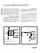
Note 6: t
PD
and t
SKEW
are measured from the 1.4V level of the output clock, to the 1.4V level of either the rising or falling edge of a
data bit. t
DCLK
is measured from the 50% level of the clock-overdrive signal on TNK+ to the 1.4V level of DCLK. The capac-
itive load on the outputs is 15pF.
GAIN = GND, open, V
CC
GAIN = open (mid gain), f
IN
= 50MHz,
-1dB below full scale
GAIN = open (mid gain)
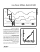
5.7
ENOB
M
5.6 5.85
Effective Number of Bits
GAIN = open (mid gain)
GAIN = GND (low gain)
Q channel
I channel
dB
CONDITIONS
MHz55BWAnalog Input -0.5dB Bandwidth
Msps90f
MAX
Maximum Sample Rate
-55XTLK
GAIN = V
CC
(high gain)
Crosstalk Between ADCs
LSB
-0.5 0.5
OFFInput Offset (Note 5)
-0.5 0.5
dB35.5 37SINAD
Signal-to-Noise plus Distortion
Ratio
Bits
5.85ENOB
L
5.8ENOB
H
(Note 5)
dB-0.2 ±0.1 0.2AM
Amplitude Match Between
ADCs
LSB-0.5 ±0.25 0.5OMMOffset Mismatch Between ADCs
(Note 6)
(Note 6)
ns1.5t
SKEW
Data Valid Skew
ns3.6t
PD
Clock to Data Propagation
Delay
degrees-2 ±0.5 2PM
UNITSMIN TYP MAXSYMBOLPARAMETER
Phase Match Between ADCs
TNK+ to DCLK (Note 6) ns5.3t
DCLK
Input to DCLK Delay
Figure 8 ns7.5t
AD
Aperture Delay
Figure 8
clock
cycle
1PDPipeline Delay
TIMING CHARACTERISTICS (Data outputs: R
L
= 1MΩ, C
L
= 15pF)
DYNAMIC PERFORMANCE (Gain = open, external 90MHz clock (Figure 7), V
INI
= V
INQ
= 20MHz sine, amplitude -1dB below
full scale, unless otherwise noted.)