
User Manual


MAX1003
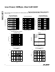
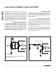
Single-ended and differential AC-coupled input circuits
are shown in Figures 2 and 3. Each of the amplifier
inputs is internally biased to a 2.35V reference through
a 20kΩ resistor, eliminating external DC bias circuits. A
series 0.1µF capacitor is required at each amplifier
input for AC-coupled signals.
When operating with AC-coupled inputs, the input
amplifiers’ DC offset voltage is nulled to within ±1/2LSB
by an on-chip offset-correction amplifier. An external
compensation capacitor is required to set the dominant
pole of the offset-correction amplifier’s frequency
response (Figures 2 and 3). The compensation capaci-
tor will determine the low-frequency corner of the ana-
log input response according to the following formula:
f
c
= 1 / (0.1 x C)
where C is the value of the compensation capacitor in
µF, and f
c
is the corner frequency in Hz.
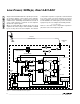
Low-Power, 90Msps, Dual 6-Bit ADC
6 _______________________________________________________________________________________
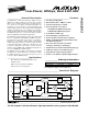
0
DIV
90Msps
DATA
BUFFER
TANK
MODCTL CAR
SYNTHESIZER
FIN
IIN
AGC
CLK IN
DSP
QIN
ADC CLOCK
6 BITS
TANK
LO
TSA5055
or EQUIV.
90
MOD GND
AGC
IOUT
QOUT
V
CC
FROM TANK VOLTAGE
VARACTOR-TUNED
PRESELECTION FILTER
EXTERNAL
VCO
OR
OR
KU BAND
75Ω CABLE
950MHz TO 2150MHz
F-CONNECTOR
INPUT
MAX2102
MAX1003
DATA
BUFFER
LO
RFIN
RFIN
LNB
6 BITS
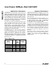
Figure 1. Commercial Satellite Receiver System