
User Manual
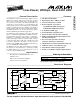


MAX1003
The MAX1003 features a proprietary encoding scheme
that ensures no more than 1LSB dynamic encoding
error. Dynamic encoding errors resulting from
metastable states may occur when the analog input
voltage, at the time the sample is taken, falls close to
the decision point for any one of the input comparators.
The resulting output code for typical converters can be
incorrect, including false full- or zero-scale outputs. The
MAX1003’s unique design reduces the magnitude of
this type of error to 1LSB.
Internal Voltage Reference
An internal buffered bandgap reference is included on
the MAX1003 to drive the ADCs’ reference ladders. The
on-chip reference and buffer eliminate any external
(high-impedance) connections to the reference ladder,
minimizing the potential for noise coupling from exter-
nal circuitry while ensuring that the voltage reference,
input amplifier, and reference ladder track well with
variations of temperature and power supplies.
Oscillator Circuit
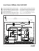
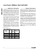
The MAX1003 includes a differential oscillator, which is
controlled by an external parallel resonant (tank) net-
work as shown in Figure 6. Alternatively, the oscillator
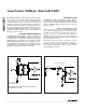
may be overdriven with an external clock source as
shown in Figure 7.
Internal Clock Operation (Tank)
If the tank circuit is used, the resonant inductor should
have a sufficiently high Q and a self-resonant frequen-
cy (SRF) of at least twice the intended oscillator fre-
quency. Coilcraft’s 1008HS-221, with an SRF of
700MHz and a Q of 45, works well for this application.
Generate different clock frequency ranges by adjusting
varactor and tank elements.
An internal clock-driver buffer is included to provide
sharp clock edges to the internal flash comparators.
The buffer ensures that the comparators are simultane-
ously clocked, maximizing the ADCs’ effective number
of bits (ENOB) performance.
Low-Power, 90Msps, Dual 6-Bit ADC
8 _______________________________________________________________________________________
Figure 6. Tank Resonator Oscillator
Figure 7. External Clock Drive Circuit
MAX1003
CLK
DRIVER
VARACTOR DIODE PAIR IS M/A-COM MA4ST079CK-287 (SOT23 PACKAGE)
INDUCTOR COILCRAFT 1008HS-221.
V
TUNE
= 0V TO 8V
f
OSC
= 70MHz TO 110MHz
TNK-
TNK+
V
TUNE
220nH
5pF
47pF
47pF
47k
47k
10k
MAX1003
CLK
DRIVER
TNK-
V
CLK
V
CLK
= 300mV
p-p
TO 1.25V
p-p
TNK+
50Ω
50Ω
Z
0
= 50Ω
50Ω
0.1µF
0.1µF