
User Manual


External Clock Operation
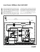
To accommodate designs that use an external clock,
the MAX1003’s internal oscillator can be overdriven by
an external clock source as shown in Figure 7. The
external clock source should be a sinusoid to minimize
clock phase noise and jitter, which can degrade the
ADCs’ ENOB performance. AC couple the clock source
(recommended voltage level is approximately 1Vp-p) to
the oscillator inputs as shown in Figure 7.
Output Data Format
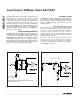
The conversion results are output on a dual, 6-bit-wide
data bus. Data is latched into the ADC output latch fol-
lowing a pipeline delay of one clock cycle, as shown in
Figure 8. Output data is clocked out of the respective
ADC’s data output pins (D_0 through D_5) on the rising
edge of the clock output (DCLK), with a DCLK-to-data
propagation delay (t
PD
) of 3.6ns. The MAX1003 outputs
are +3.3V CMOS-logic compatible.
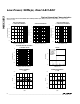
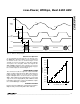
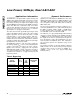
Transfer Function
Figure 9 shows the MAX1003’s nominal transfer function.
Output coding is offset binary with 1LSB = FSR / 63.
MAX1003
Low-Power, 90Msps, Dual 6-Bit ADC
_______________________________________________________________________________________ 9
Figure 9. Ideal Transfer Function
111111
OUTPUT CODE
111110
111101
100001
100000
011111
011110
000011
000010
000001
000000
-FSR
2
0
1LSB
INPUT VOLTAGE (_IN+ TO _IN-)
FSR
2
Figure 8. MAX1003 Timing Diagram
DATA OUT
1.4V
DATA VALID N - 1 DATA VALID N
1.4V
50%
t
SKEW
t
DCLK
t
AD
t
PD
TNK+
(INPUT CLOCK)
DCLK
ANALOG
INPUT
N
N + 1
N + 2