
User guide

MAX1027/MAX1029/MAX1031
10-Bit 300ksps ADCs with FIFO,
Temp Sensor, Internal Reference
2 _______________________________________________________________________________________
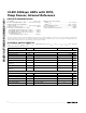
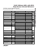
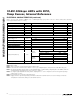
ABSOLUTE MAXIMUM RATINGS
ELECTRICAL CHARACTERISTICS
(V
DD
= +2.7V to +3.6V, f
SAMPLE
= 300kHz, f
SCLK
= 4.8MHz (50% duty cycle), V
REF
= 2.5V, T
A
= T
MIN
to T
MAX
, unless otherwise
noted. Typical values are at T
A
= +25°C.)
Stresses beyond those listed under “Absolute Maximum Ratings” may cause permanent damage to the device. These are stress ratings only, and functional
operation of the device at these or any other conditions beyond those indicated in the operational sections of the specifications is not implied. Exposure to
absolute maximum rating conditions for extended periods may affect device reliability.
V
DD
to GND..............................................................-0.3V to +6V
CS, SCLK, DIN, EOC, DOUT to GND.........-0.3V to (V
DD
+ 0.3V)
AIN0–AIN13, REF-/AIN_, CNVST/AIN_,
REF+ to GND.........................................-0.3V to (V
DD
+ 0.3V)
Maximum Current into Any Pin............................................50mA
Continuous Power Dissipation (T
A
= +70°C)
16-Pin QSOP (derate 8.3mW/°C above +70°C)...........667mW
20-Pin QSOP (derate 9.1mW/°C above +70°C)...........727mW
24-Pin QSOP (derate 9.5mW/°C above +70°C)...........762mW
28-Pin QFN 5mm x 5mm
(derate 20.8mW/°C above +70°C)........................1667mW
Operating Temperature Ranges
MAX10__C__.......................................................0°C to +70°C
MAX10__E__....................................................-40°C to +85°C
Storage Temperature Range .............................-60°C to +150°C
Junction Temperature......................................................+150°C
Lead Temperature (soldering, 10s) .................................+300°C
PARAMETER SYMBOL CONDITIONS MIN TYP MAX UNITS
DC ACCURACY (Note 1)
Resolution RES 10 Bits
Integral Nonlinearity INL ±1.0 LSB
Differential Nonlinearity DNL No missing codes over temperature ±1.0 LSB
Offset Error ±0.5 ±2.0 LSB
Gain Error (Note 2) ±0.5 ±2.0 LSB
Offset Error Temperature
Coefficient
±2
ppm/°C
FSR
Gain Temperature Coefficient ±0.8 ppm/°C
Channel-to-Channel Offset
Matching
±0.1 LSB
DYNAMIC SPECIFICATIONS (10kHz sine wave input, 2.5V
P-P
, 300ksps, f
SCLK
= 4.8MHz)
Signal-to-Noise Plus Distortion SINAD 70 dB
Total Harmonic Distortion THD Up to the 5th harmonic -82 dBc
Spurious-Free Dynamic Range SFDR 80 dBc
Intermodulation Distortion IMD f
in1
= 9.9kHz, f
in2
= 10.2kHz 76 dBc
Full-Power Bandwidth -3dB point 1 MHz
Full-Linear Bandwidth S / (N + D) > 68dB 25 kHz