
User guide

MAX1027/MAX1029/MAX1031
10-Bit 300ksps ADCs with FIFO,
Temp Sensor, Internal Reference
_______________________________________________________________________________________ 3
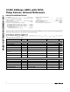
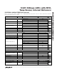
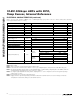
ELECTRICAL CHARACTERISTICS (continued)
(V
DD
= +2.7V to +3.6V, f
SAMPLE
= 300kHz, f
SCLK
= 4.8MHz (50% duty cycle), V
REF
= 2.5V, T
A
= T
MIN
to T
MAX
, unless otherwise
noted. Typical values are at T
A
= +25°C.)
PARAMETER SYMBOL CONDITIONS MIN TYP MAX UNITS
CONVERSION RATE
External reference 0.8
Power-Up Time t
PU
Internal reference (Note 3) 65
µs
Acquisition Time t
ACQ
0.6 µs
Internally clocked 3.5
Conversion Time t
CONV
Externally clocked (Note 4) 2.7
µs
Externally clocked conversion 0.1 4.8
External Clock Frequency f
SCLK
Data I/O 10
MHz
SCLK Duty Cycle 40 60 %
Aperture Delay 30 ns
Aperture Jitter <50 ps
ANALOG INPUT
Unipolar 0 V
REF
Input Voltage Range
Bipolar (Note 5) - V
RE F
/ 2 V
RE F
/ 2
V
Input Leakage Current V
IN
= V
DD
±0.01 ±1 µA
Input Capacitance During acquisition time (Note 6) 24 pF
INTERNAL TEMPERATURE SENSOR
Grade A, T
A
= +25°C ±0.3
Grade A, T
A
= -20°C to +85°C ±0.5 ±1
Grade A, T
A
= T
MIN
to T
MAX
±0.75 ±1.5
Grade B, T
A
= +25°C ±0.7
Measurement Error (Note 7)
Grade B, T
A
= T
MIN
to T
MAX
±1.2 ±2.5
°C
Temperature Measurement Noise 0.1 °C
RMS
Temperature Resolution 1/8 °C
Power-Supply Rejection 0.3 °C/V
INTERNAL REFERENCE
REF Output Voltage 2.48 2.50 2.52 V
Grade A ±8
REF Temperature Coefficient TC
REF
Grade B ±30
ppm/°C
Output Resistance 6.5 kΩ
REF Output Noise 200 µV
RMS
REF Power-Supply Rejection PSRR -70 dB
EXTERNAL REFERENCE INPUT
REF- Input Voltage Range V
REF-
0 500 mV
REF+ Input Voltage Range V
REF+
1.0 V
DD
+ 50mV V
V
REF+
= 2.5V, f
SAMPLE
= 300ksps 40 100
REF+ Input Current I
REF+
V
REF+
= 2.5V, f
SAMPLE
= 0 ±0.1 ±5
µA