
User guide

MAX1027/MAX1029/MAX1031
10-Bit 300ksps ADCs with FIFO,
Temp Sensor, Internal Reference
4 _______________________________________________________________________________________
Note 1: Tested at V
DD
= +2.7V, unipolar input mode.
Note 2: Offset nulled.
Note 3: Time for reference to power up and settle to within 1 LSB.
Note 4: Conversion time is defined as the number of clock cycles multiplied by the clock period; clock has 50% duty cycle.
Note 5: The operational input voltage range for each individual input of a differentially configured pair is from GND to V
DD
. The
operational input voltage difference is from -V
REF
/ 2 to +V
REF
/ 2.
Note 6: See Figure 3 (Input Equivalent Circuit) and the Sampling Error vs. Source Impedance curve in the Typical Operating
Characteristics section.
Note 7: Fast automated test, excludes self-heating effects.
Note 8: Supply current is specified depending on whether an internal or external reference is used for voltage conversions.
Temperature measurements always use the internal reference.
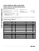
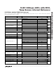
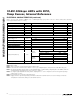
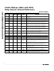
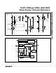
ELECTRICAL CHARACTERISTICS (continued)
(V
DD
= +2.7V to +3.6V, f
SAMPLE
= 300kHz, f
SCLK
= 4.8MHz (50% duty cycle), V
REF
= 2.5V, T
A
= T
MIN
to T
MAX
, unless otherwise
noted. Typical values are at T
A
= +25°C.)
PARAMETER SYMBOL CONDITIONS MIN TYP MAX UNITS
DIGITAL INPUTS (SCLK, DIN, CS, CNVST)
Input Voltage Low V
IL
V
DD
x 0.3 V
Input Voltage High V
IH
V
DD
x 0.7 V
Input Hysteresis V
HYST
200 mV
Input Leakage Current I
IN
V
IN
= 0 or V
DD
±0.01 ±1.0 µA
Input Capacitance C
IN
15 pF
DIGITAL OUTPUTS (DOUT, EOC)
I
SINK
= 2mA 0.4
Output Voltage Low V
OL
I
SINK
= 4mA 0.8
V
Output Voltage High V
OH
I
SOURCE
= 1.5mA V
DD
- 0.5 V
Tri-State Leakage Current I
L
CS = V
DD
±0.05 ±1 µA
Tri-State Output Capacitance C
OUT
CS = V
DD
15 pF
POWER REQUIREMENTS
Supply Voltage V
DD
2.7 3.6 V
During temp sense 2200 2700
f
SAMPLE
= 300ksps 1550 1800
f
SAMPLE
= 0, REF on 1000 1200
Internal
reference
Shutdown 0.2 5
During temp sense 1550 2000
f
SAMPLE
= 300ksps 880 1100
Supply Current (Note 8) I
DD
External
reference
Shutdown 0.2 5
µA
Power-Supply Rejection PSR V
DD
= 2.7V to 3.6V; full-scale input ±0.2 ±1 mV