
User guide

MAX1027/MAX1029/MAX1031
10-Bit 300ksps ADCs with FIFO,
Temp Sensor, Internal Reference
8 _______________________________________________________________________________________
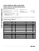
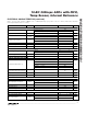
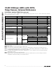
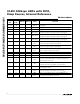
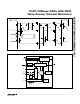
Pin Description
MAX1031
QFN
MAX1031
QSOP
MAX1029 MAX1027 NAME FUNCTION
2–12, 26,
27, 28
1–14 ——AIN0–13 Analog Inputs
——1–10 — AIN0–9 Analog Inputs
———1–6AIN0–5 Analog Inputs
13 15 ——REF-/AIN14
Negative Input for External Differential Reference/Analog Input 14.
See Table 3 for details on programming the setup register.
——11 — REF-/AIN10
Negative Input for External Differential Reference/Analog Input 10.
See Table 3 for details on programming the setup register.
——— 7 REF-/AIN6
Negative Input for External Differential Reference/Analog Input 6.
See Table 3 for details on programming the setup register.
14 16 ——
CNVST/
AIN15
Active-Low Conversion Start Input/Analog Input 15. See Table 3
for details on programming the setup register.
——12 —
CNVST/
AIN11
Active-Low Conversion Start Input/Analog Input 11. See Table 3
for details on programming the setup register.
——— 8
CNVST/
AIN7
Active-Low Conversion Start Input/Analog Input 7. See Table 3 for
details on programming the setup register.
15 17 13 9 REF+ Positive Reference Input. Bypass to GND with a 0.1µF capacitor.
16 18 14 10 GND Ground
18 19 15 11 V
DD
Power Input. Bypass to GND with a 0.1µF capacitor.
20 20 16 12 SCLK
Serial Clock Input. Clocks data in and out of the serial interface.
(Duty cycle must be 40% to 60%.) See Table 3 for details on
programming the clock mode.
21 21 17 13 CS
Active-Low Chip Select Input. When CS is low, the serial interface
is enabled. When CS is high, DOUT is high impedance.
22 22 18 14 DIN
Serial Data Input. DIN data is latched into the serial interface on
the rising edge of SCLK.
23 23 19 15 DOUT
Serial Data Output. Data is clocked out on the falling edge of
SCLK. High impedance when CS is connected to V
DD
.
24 24 20 16 EOC End of Conversion Output. Data is valid after EOC pulls low.
1, 17, 19,
25
———N.C. No Connection. Not internally connected.