
Owner manual
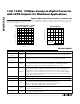


Digital Outputs (D0P/N–D9P/N, DCLKP/N,
ORP/N) and Control Input
T
/B
The digital outputs D0P/N–D9P/N, DCLKP/N, and
ORP/N are LVDS compatible, and data on
D0P/N–D9P/N is presented in either binary or two’s
complement format (Table 1). The T/B control line is an
LVCMOS-compatible input, which allows the user to
select the desired output format. Pulling T/B low out-
puts data in two’s complement and pulling it high pre-
sents data in offset binary format on the 10-bit parallel
bus. T/B has an internal pulldown resistor and may be
left unconnected in applications using only two’s com-
plement output format. All LVDS outputs provide a typi-
cal voltage swing of 0.4V around a common-mode
voltage of approximately 1.2V, and must be terminated
at the far end of each transmission line pair (true and
complementary) with 100Ω. The LVDS outputs are pow-
ered from a separate power supply, which can be
operated between 1.7V and 1.9V.
The MAX1122 offers an additional differential output
pair (ORP, ORN) to flag out-of-range conditions, where
out of range is above positive or below negative full
scale. An out-of-range condition is identified with ORP
(ORN) transitioning high (low).
Note: Although differential LVDS reduces single-ended
transients to the supply and ground planes, capacitive
loading on the digital outputs should still be kept as low
as possible. Using LVDS buffers on the digital outputs
of the ADC when driving off-board may improve overall
performance and reduce system timing constraints.
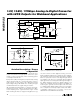
Applications Information
Full-Scale Range Adjustments Using the
Internal Bandgap Reference
The MAX1122 supports a full-scale adjustment range of
10% (±5%). To decrease the full-scale range, an exter-
nal resistor value ranging from 13kΩ to 1MΩ may be
added between REFADJ and AGND. A similar
approach can be taken to increase the ADCs full-scale
range. Adding a variable resistor, potentiometer, or
MAX1122
1.8V, 10-Bit, 170Msps Analog-to-Digital Converter
with LVDS Outputs for Wideband Applications
______________________________________________________________________________________ 13
REFERENCE
BUFFER
REFIO
REFADJ
AV
CC
AV
CC
/ 2
CONTROL LINE TO
DISABLE REFERENCE
BUFFER
ADC FULL-SCALE = REFT - REFB
G
1V
0.1µF
REFERENCE-
SCALING
AMPLIFIER
REFT
REFB
13kΩ TO 1MΩ
13kΩ TO 1MΩ
Figure 6. Circuit Suggestions to Adjust the ADC’s Full-Scale
Range
MAX1122
50Ω
CLKPCLKN
SINGLE-ENDED
INPUT TERMINAL
MC100LVEL16
510Ω510Ω
150Ω
150Ω
V
CLK
VGND
2
3
45
6
7
8
0.1µF
0.1µF
0.1µF
0.1µF
0.01µF
10
D0P/N–D9P/N
AV
CC
OV
CC
AGND OGND
INP
INN
Figure 7. Differential, AC-Coupled, PECL-Compatible Clock Input Configuration