
Owner manual


MAX1122
predetermined resistor value between REFADJ and
REFIO increases the full-scale range of the data con-
verter. Figure 6 shows the two possible configurations
and their impact on the overall full-scale range adjust-
ment of the MAX1122. Do not use resistor values of less
than 13kΩ to avoid instability of the internal gain regula-
tion loop for the bandgap reference.
Differential, AC-Coupled, PECL-Compatible
Clock Input
The preferred method of clocking the MAX1122 is differ-
entially with LVDS- or PECL-compatible input levels. To
accomplish this, a 50Ω reverse-terminated clock signal
source with low phase noise is AC-coupled into a fast
differential receiver such as the MC100LVEL16 (Figure
7). The receiver produces the necessary PECL output
levels to drive the clock inputs of the data converter.
Differential, AC-Coupled Analog Input
An RF transformer provides an excellent solution to
convert a single-ended source signal to a fully differen-
tial signal, required by the MAX1122 for optimum
dynamic performance. In general, the MAX1122 pro-
vides the best SFDR and THD with fully differential
input signals and it is not recommended to drive the
ADC inputs in single-ended configuration. In differential
input mode, even-order harmonics are usually lower
since INP and INN are balanced, and each of the ADC
inputs only requires half the signal swing compared to
a single-ended configuration.
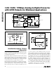
Figure 8 depicts a secondary-side termination of the 1:1
transformer into two separate 25Ω loads. Terminating the
transformer in this fashion reduces the potential effects of
transformer parasitics. The source impedance combined
with the shunt capacitance provided by a PC board and
the ADC’s parasitic capacitance reduce the combined
bandwidth to approximately 550MHz.
Single-Ended, AC-Coupled Analog Input
Although not recommended, the MAX1122 can be
used in single-ended mode (Figure 9). Analog signals
can be AC-coupled to the positive input INP through a
0.1µF capacitor and terminated with a 50Ω resistor to
AGND. The negative input should be 25Ω reverse-
terminated and AC grounded with a 0.1µF capacitor.
Grounding, Bypassing, and Board
Layout Considerations
The MAX1122 requires board layout design techniques
suitable for high-speed data converters. This ADC pro-
vides separate analog and digital power supplies. The
analog and digital supply voltage pins accept input
voltage ranges of 1.7V to 1.9V. Although both supply
types can be combined and supplied from one source,
it is recommended to use separate sources to cut down
on performance degradation caused by digital switch-
ing currents, which can couple into the analog supply
network. Isolate analog and digital supplies (AV
CC
and
OV
CC
) where they enter the PC board with separate
1.8V, 10-Bit, 170Msps Analog-to-Digital Converter
with LVDS Outputs for Wideband Applications
14 ______________________________________________________________________________________
MAX1122
10
D0P/N–D9P/N
AV
CC
OV
CC
AGND OGND
INP
INN
25Ω
25Ω
15Ω
15Ω
ADT1–1WT
0.1µF
0.1µF
SINGLE-ENDED
INPUT TERMINAL
Figure 8. Transformer-Coupled Analog Input Configuration with Secondary-Side Termination
MAX1122
10
D0P/N–D9P/N
AV
CC
OV
CC
AGND OGND
0.1µF
SINGLE-ENDED
INPUT TERMINAL
0.1µF
INP
INN
50Ω
25Ω
Figure 9. Single-Ended AC-Coupled Analog Input
Configuration