
Owner manual

MAX1122
1.8V, 10-Bit, 170Msps Analog-to-Digital Converter
with LVDS Outputs for Wideband Applications
_______________________________________________________________________________________ 3
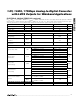
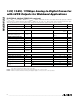
ELECTRICAL CHARACTERISTICS (continued)
(AV
CC
= OV
CC
= 1.8V, AGND = OGND = 0, f
SAMPLE
= 170MHz, differential sine-wave clock input drive, 0.1µF capacitor on REFIO,
internal reference, digital output pins differential R
L
= 100Ω ±1%, C
L
= 5pF, T
A
= T
MIN
to T
MAX
, unless otherwise noted. ≥25°C guar-
anteed by production test, <25°C guaranteed by design and characterization. Typical values are at T
A
= +25°C.)
PARAMETER
SYMBOL
CONDITIONS
MIN
TYP
MAX
UNITS
Clock Duty Cycle Set by clock management circuit
40 to 60
%
Aperture Delay t
AD
350
ps
Aperture Jitter t
AJ
0.2
ps
RMS
CLOCK INPUTS (CLKP, CLKN)
Differential Clock Input Amplitude
(Note 2)
200 500
mV
P-P
Clock Input Common-Mode
Voltage Range
1.15
±0.25
V
Clock Differential Input
Resistance
R
CLK
11 ±
25%
kΩ
Clock Differential Input
Capacitance
C
CLK
5pF
DYNAMIC CHARACTERISTICS (at -0.5dBFS)
f
IN
= 10MHz, T
A
≥ +25°C
56.5 57.5
f
IN
= 100MHz, T
A
≥ +25°C
55.5 57.1
f
IN
= 180MHz
57.1
Signal-to-Noise Ratio SNR
f
IN
= 500MHz
56.5
dB
f
IN
= 10MHz, T
A
≥ +25°C56
57.4
f
IN
= 100MHz, T
A
≥ +25°C5557
f
IN
= 180MHz
56.7
Signal-to-Noise
and Distortion
SINAD
f
IN
= 500MHz
55.3
dB
f
IN
= 10MHz, T
A
≥ +25°C6577
f
IN
= 100MHz, T
A
≥ +25°C6472
f
IN
= 180MHz 67
Spurious-Free
Dynamic Range
SFDR
f
IN
= 500MHz
63.5
dBc
f
IN
= 10MHz -77
f
IN
= 100MHz -72
f
IN
= 180MHz -67
Worst Harmonics
(HD2 or HD3)
f
IN
= 500MHz
-63.5
dBc
IMD
100
f
IN1
= 99MHz at -7dBFS,
f
IN2
= 101MHz at -7dBFS
-79
Two-Tone Intermodulation
Distortion
IMD
500
f
IN1
= 499MHz at -7dBFS,
f
IN2
= 503MHz at -7dBFS
-60
dBc
LVDS DIGITAL OUTPUTS (D0P/N–D9P/N, DCLKP/N)
Differential Output Voltage |V
OD
|
250 400
mV