
Owner manual

MAX1122
1.8V, 10-Bit, 170Msps Analog-to-Digital Converter
with LVDS Outputs for Wideband Applications
4 _______________________________________________________________________________________
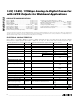
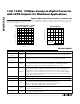
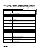
ELECTRICAL CHARACTERISTICS (continued)
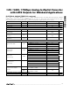
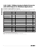
(AV
CC
= OV
CC
= 1.8V, AGND = OGND = 0, f
SAMPLE
= 170MHz, differential sine-wave clock input drive, 0.1µF capacitor on REFIO,
internal reference, digital output pins differential R
L
= 100Ω ±1%, C
L
= 5pF, T
A
= T
MIN
to T
MAX
, unless otherwise noted. ≥25°C guar-
anteed by production test, <25°C guaranteed by design and characterization. Typical values are at T
A
= +25°C.)
PARAMETER
SYMBOL
CONDITIONS
MIN TYP MAX
UNITS
Output Offset Voltage OV
OS
1.125 1.310
V
LVCMOS DIGITAL INPUTS (CLKDIV, T/B)
Digital Input Voltage Low V
IL
0.2 x
AV
CC
V
Digital Input Voltage High V
IH
0.8 x
AV
CC
V
TIMING CHARACTERISTICS
CLK to Data Propagation Delay t
PDL
Figure 4 1.5 ns
CLK to DCLK Propagation Delay
t
CPDL
Figure 4
3.43
ns
Data Valid to DCLK Rising Edge
t
CPDL
-
t
ADL
Figure 4 (Note 2)
1.67 1.93 2.35
ns
LVDS Output Rise-Time t
RISE
20% to 80%, C
L
= 5pF
460
ps
LVDS Output Fall-Time t
FALL
20% to 80%, C
L
= 5pF
460
ps
Output Data Pipeline Delay
t
LATENCY
8
Clock
cycles
POWER REQUIREMENTS
Analog Supply Voltage Range AV
CC
1.7 1.8 1.9 V
Digital Supply Voltage Range OV
CC
1.7 1.8 1.9 V
Analog Supply
I
AVCC
f
IN
= 100MHz
210 275
mA
Digital Supply Current I
OVCC
f
IN
= 100MHz 45 75 mA
Analog Power Dissipation P
DISS
f
IN
= 100MHz
460 630
mW
Offset 1.6
mV/V
Power-Supply Rejection Ratio
(Note 3)
PSRR
Gain 1.9
%FS/V
Note 1: Static linearity and offset parameters are computed from a best-fit straight line through the code transition points. The full-
scale range is defined as 1023 x slope of the line.
Note 2: Parameter guaranteed by design and characterization; T
A
= T
MIN
to T
MAX
.
Note 3: PSRR is measured with both analog and digital supplies connected to the same potential.