
Owner manual

MAX1122
1.8V, 10-Bit, 170Msps Analog-to-Digital Converter
with LVDS Outputs for Wideband Applications
8 _______________________________________________________________________________________
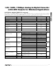
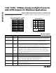
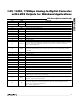
Pin Description
PIN NAME FUNCTION
1, 6, 11–14, 20, 25,
62, 63, 65
AV
CC
Analog Supply Voltage. Bypass each pin with a 0.1µF capacitor for best decoupling results.
2, 5, 7, 10, 15, 16,
18, 19, 21, 24, 64,
66, 67, EP
AGND Analog Converter Ground. Connect the converter’s exposed paddle (EP) to AGND.
3 REFIO
Reference Input/Output. With REFADJ pulled high through a 1kΩ resistor, this I/O port allows
an external reference source to be connected to the MAX1122. With REFADJ pulled low
through the same 1kΩ resistor, the internal 1.23V bandgap reference is active.
4 REFADJ
Reference-Adjust Input. REFADJ allows for full-scale range adjustments by placing a resistor
or trim potentiometer between REFADJ and AGND (decreases FS range) or REFADJ and
REFIO (increases FS range). If REFADJ is connected to AV
CC
through a 1kΩ resistor, the
internal reference can be overdriven with an external source connected to REFIO. If REFADJ
is connected to AGND through a 1kΩ resistor, the internal reference is used to determine the
full-scale range of the data converter.
8 INP Positive Analog Input Terminal
9INN Negative Analog Input Terminal
17 CLKDIV
Clock Divider Input. This LVCMOS-compatible input controls which speed the converter’s
digital outputs are updated. CLKDIV has an internal pulldown resistor.
CLKDIV = 0: ADC updates digital outputs at one-half the input clock rate.
CLKDIV = 1: ADC updates digital outputs at the input clock rate.
22 CLKP
True Clock Input. This input requires an LVDS-compatible input level to maintain the
converter’s excellent performance.
23 CLKN
Complementary Clock Input. This input requires an LVDS-compatible input level to maintain
the converter’s excellent performance.
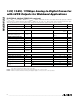
50
58
57
59
55
54
56
52
51
53
60
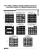
30 48 5436 42 60 66 72
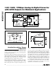
SINAD vs. CLOCK DUTY CYCLE (f
IN
= 1.4006MHz,
f
SAMPLE
= 169.984MHz, A
IN
= -0.5dBFS)
MAX1122 toc27
CLOCK DUTY CYCLE (%)
SINAD (dB)
-100
-80
-90
-60
-70
-50
-40
5101520253035
NOISE POWER RATIO PLOT
MAX1122 toc28
ANALOG INPUT FREQUENCY (MHz)
POWER SPECTRAL DENSITY (dB)
f
SAMPLE
= 170MHz
f
NOTCH
= 28.8MHz
NPR = 53.7dB
Typical Operating Characteristics (continued)
(AV
CC
= OV
CC
= 1.8V, AGND = OGND = 0, f
SAMPLE
= 170.0057MHz, -0.5dBFS; see TOCs for detailed information on test condi-
tions, differential input drive, differential sine-wave clock input drive, 0.1µF capacitor on REFIO, internal reference, digital output pins
differential R
L
= 100Ω, T
A
= +25°C.)