9-3143; Rev 0; 1/04 KIT ATION EVALU LE B A IL A AV Quad, 12-Bit, 40Msps, 1.8V ADC with Serial LVDS Outputs Features The MAX1126 quad, 12-bit analog-to-digital converter (ADC) features fully differential inputs, a pipelined architecture, and digital error correction. This ADC is optimized for low-power, high-dynamic performance for medical imaging, communications, and instrumentation applications. The MAX1126 operates from a 1.7V to 1.9V single supply and consumes only 563mW while delivering a 69.
MAX1126 Quad, 12-Bit, 40Msps, 1.8V ADC with Serial LVDS Outputs ABSOLUTE MAXIMUM RATINGS T/B, LVDSTEST to GND ...........................-0.3V to (AVDD + 0.3V) REFIO, INTREF to GND............................-0.3V to (AVDD + 0.3V) I.C. to GND...............................................-0.3V to (AVDD + 0.3V) Continuous Power Dissipation (TA = +70°C) 68-Pin QFN 10mm x 10mm x 0.9mm (derated 41.7mW/°C above +70°C)........................3333.3mW Operating Temperature Range ...........................
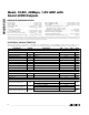
Quad, 12-Bit, 40Msps, 1.8V ADC with Serial LVDS Outputs (AV DD = 1.8V, OV DD = 1.8V, CV DD = 1.8V, GND = 0, external V REFIO = 1.24V, INTREF = AV DD, C REFIO to GND = 0.1µF, fCLK = 40MHz (50% duty cycle), DT = 0, TA = TMIN to TMAX, unless otherwise noted. Typical values are at TA = +25°C.) (Note 1) PARAMETER SYMBOL Spurious-Free Dynamic Range (Note 2) SFDR Total Harmonic Distortion (Note 2) THD Intermodulation Distortion Third-Order Intermodulation CONDITIONS MIN fIN = 5.3MHz at -0.5dBFS fIN = 19.
MAX1126 Quad, 12-Bit, 40Msps, 1.8V ADC with Serial LVDS Outputs ELECTRICAL CHARACTERISTICS (continued) (AV DD = 1.8V, OV DD = 1.8V, CV DD = 1.8V, GND = 0, external V REFIO = 1.24V, INTREF = AV DD, C REFIO to GND = 0.1µF, fCLK = 40MHz (50% duty cycle), DT = 0, TA = TMIN to TMAX, unless otherwise noted. Typical values are at TA = +25°C.
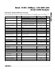
Quad, 12-Bit, 40Msps, 1.8V ADC with Serial LVDS Outputs (AV DD = 1.8V, OV DD = 1.8V, CV DD = 1.8V, GND = 0, external V REFIO = 1.24V, INTREF = AV DD, C REFIO to GND = 0.1µF, fCLK = 40MHz (50% duty cycle), DT = 0, TA = TMIN to TMAX, unless otherwise noted. Typical values are at TA = +25°C.) (Note 1) PARAMETER SYMBOL AVDD Supply Current OVDD Supply Current IAVDD IOVDD CONDITIONS fIN = 19.3MHz at -0.5dBFS fIN = 19.3MHz at -0.
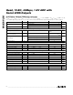
MAX1126 Quad, 12-Bit, 40Msps, 1.8V ADC with Serial LVDS Outputs ELECTRICAL CHARACTERISTICS (continued) (AV DD = 1.8V, OV DD = 1.8V, CV DD = 1.8V, GND = 0, external V REFIO = 1.24V, INTREF = AV DD, C REFIO to GND = 0.1µF, fCLK = 40MHz (50% duty cycle), DT = 0, TA = TMIN to TMAX, unless otherwise noted. Typical values are at TA = +25°C.) (Note 1) PARAMETER SYMBOL CONDITIONS MIN TYP MAX UNITS CHANNEL-TO-CHANNEL MATCHING Crosstalk (Note 2) -90 dB Gain Matching fIN = 19.3MHz (Note 2) ±0.
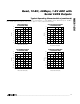
Quad, 12-Bit, 40Msps, 1.8V ADC with Serial LVDS Outputs FFT PLOT (32,768-POINT DATA RECORD) -40 -50 -60 -70 -80 -90 -100 HD3 HD2 -110 -120 fCLK = 40.96MHz fIN = 19.00125MHz AIN = -0.5dBFS SNR = 69.20dB SINAD = 69.16dB THD = -88.74dBc SFDR = 89.
Typical Operating Characteristics (continued) (AVDD = 1.8V, OVDD = 1.8V, CVDD = 1.8V, GND = 0, external VREFIO = 1.24V, INTREF = AVDD, differential input at -0.5dBFS, fCLK = 40MHz (50% duty cycle), DT = low, CLOAD = 10pF, TA = +25°C, unless otherwise noted.) SIGNAL-TO-NOISE PLUS DISTORTION vs. ANALOG INPUT FREQUENCY SIGNAL-TO-NOISE RATIO vs.
Quad, 12-Bit, 40Msps, 1.8V ADC with Serial LVDS Outputs SIGNAL-TO-NOISE RATIO vs. ANALOG INPUT POWER SIGNAL-TO-NOISE PLUS DISTORTION vs. ANALOG INPUT POWER fIN = 5.301935MHz 67 62 57 57 SINAD (dB) 62 52 47 52 47 42 42 37 37 32 32 -25 -20 -15 -10 -5 0 -25 -20 -15 -10 -5 ANALOG INPUT POWER (dBFS) TOTAL HARMONIC DISTORTION vs. ANALOG INPUT POWER SPURIOUS-FREE DYNAMIC RANGE vs. ANALOG INPUT POWER fIN = 5.
Typical Operating Characteristics (continued) (AVDD = 1.8V, OVDD = 1.8V, CVDD = 1.8V, GND = 0, external VREFIO = 1.24V, INTREF = AVDD, differential input at -0.5dBFS, fCLK = 40MHz (50% duty cycle), DT = low, CLOAD = 10pF, TA = +25°C, unless otherwise noted.) SIGNAL-TO-NOISE PLUS DISTORTION vs. SAMPLING RATE SIGNAL-TO-NOISE RATIO vs. SAMPLING RATE 70 70 69 SINAD (dB) 68 67 66 68 67 66 65 65 64 64 63 63 62 62 20 25 30 35 20 40 25 30 35 fCLK (MHz) fCLK (MHz) TOTAL HARMONIC DISTORTION vs.
Quad, 12-Bit, 40Msps, 1.8V ADC with Serial LVDS Outputs SIGNAL-TO-NOISE RATIO vs. CLOCK DUTY CYCLE 70 70 69 SINAD (dB) 68 67 66 68 67 66 65 65 64 64 63 63 62 62 30 40 50 60 70 30 40 50 60 CLOCK DUTY CYCLE (%) CLOCK DUTY CYCLE (%) TOTAL HARMONIC DISTORTION vs. CLOCK DUTY CYCLE SPURIOUS-FREE DYNAMIC RANGE vs. CLOCK DUTY CYCLE 100 MAX1126 toc22 -75 fIN = 5.301935MHz -80 fIN = 5.301935MHz 95 -85 70 MAX1126 toc23 SNR (dB) fIN = 5.
Typical Operating Characteristics (continued) (AVDD = 1.8V, OVDD = 1.8V, CVDD = 1.8V, GND = 0, external VREFIO = 1.24V, INTREF = AVDD, differential input at -0.5dBFS, fCLK = 40MHz (50% duty cycle), DT = low, CLOAD = 10pF, TA = +25°C, unless otherwise noted.) SIGNAL-TO-NOISE RATIO vs. TEMPERATURE 68 66 64 68 66 64 62 62 -15 10 35 60 -40 -15 10 35 60 TEMPERATURE (°C) TEMPERATURE (°C) TOTAL HARMONIC DISTORTION vs. TEMPERATURE SPURIOUS-FREE DYNAMIC RANGE vs.
Quad, 12-Bit, 40Msps, 1.8V ADC with Serial LVDS Outputs ANALOG SUPPLY CURRENT vs. SAMPLING RATE 260 MAX1126 toc29 70 MAX1126 toc28 270 DIGITAL SUPPLY CURRENT vs. SAMPLING RATE 60 IOVDD (mA) IAVDD (mA) 50 250 240 40 30 20 230 10 0 220 25 30 35 40 30 35 OFFSET ERROR vs. TEMPERATURE GAIN ERROR vs. TEMPERATURE 1.0 MAX1126 toc30 0.015 0.9 0.8 GAIN ERROR (%FS) 0.010 0.005 0 -0.005 -0.010 40 0.7 0.6 0.5 0.4 0.3 0.2 -0.015 0.1 -0.
Typical Operating Characteristics (continued) (AVDD = 1.8V, OVDD = 1.8V, CVDD = 1.8V, GND = 0, external VREFIO = 1.24V, INTREF = AVDD, differential input at -0.5dBFS, fCLK = 40MHz (50% duty cycle), DT = low, CLOAD = 10pF, TA = +25°C, unless otherwise noted.) 1.40 MAX1126 toc35 1.26 MAX1126 toc34 1.239 INTERNAL REFERENCE VOLTAGE vs. REFERENCE LOAD CURRENT INTERNAL REFERENCE VOLTAGE vs. TEMPERATURE 1.35 VREFIO (V) VREFIO (V) 1.237 NEGATIVE CURRENT FLOWS INTO REFIO 1.30 1.25 1.
Quad, 12-Bit, 40Msps, 1.8V ADC with Serial LVDS Outputs PIN NAME FUNCTION 29 SLVS/LVDS 30 PLL0 PLL Control Input 0. PLL0 is reserved for factory testing only and must always be connected to GND. 31 PLL1 PLL Control Input 1. PLL1 is reserved for factory testing only and must always be connected to GND. 32 PLL2 PLL Control Input 2. See Table 1 for details. 33 PLL3 PLL Control Input 3. See Table 1 for details. 34, 37, 40, 43, 46, 49, 52 OVDD Output-Driver Power Input. Connect OVDD to a 1.
MAX1126 Quad, 12-Bit, 40Msps, 1.8V ADC with Serial LVDS Outputs Pin Description (continued) PIN NAME FUNCTION 64 LVDSTEST LVDS Test Pattern Enable Input. Drive LVDSTEST high to enable the output test pattern (000010111101 MSB→LSB). As with the analog conversion results, the test pattern data is output LSB first. Drive LVDSTEST low for normal operation. 66 REFIO Reference Input/Output. For internal reference operation (INTREF = GND), the reference output voltage is 1.24V.
Quad, 12-Bit, 40Msps, 1.8V ADC with Serial LVDS Outputs The MAX1126 ADC features fully differential inputs, a pipelined architecture, and digital error correction for high-speed signal conversion. The ADC pipeline architecture moves the samples taken at the inputs through the pipeline stages every half clock cycle. The converted digital results are serialized and sent through the LVDS/SLVS output drivers. The total latency from input to output is 6.5 input clock cycles.
MAX1126 Quad, 12-Bit, 40Msps, 1.8V ADC with Serial LVDS Outputs Reference Configurations (REFIO and INTREF) The MAX1126 provides an internal 1.24V bandgap reference or can be driven with an external reference voltage. The MAX1126 full-scale analog differential input range is ±FSR. Full-scale range (FSR) is given by the following equation: V FSR = 700mV x REFIO 1.24 V where VREFIO is the voltage at REFIO, generated internally or externally. For a VREFIO = 1.24V, the full-scale input range is ±700mV (1.
Quad, 12-Bit, 40Msps, 1.8V ADC with Serial LVDS Outputs MAX1126 N+2 (VIN_P VIN_N) N+6 N+3 N N+8 N+5 N+1 N+9 N+7 N+4 tSAMPLE CLK 6.5 CLOCK-CYCLE DATA LATENCY (VFRAMEP VFRAMEN)* (VCLKOUTP VCLKOUTN) (VOUT_P VOUT_N) OUTPUT DATA FOR SAMPLE N-6 OUTPUT DATA FOR SAMPLE N *DUTY CYCLE VARIES DEPENDING ON INPUT CLOCK FREQUENCY. Figure 3.
MAX1126 Quad, 12-Bit, 40Msps, 1.8V ADC with Serial LVDS Outputs Frame Alignment Output (FRAMEP, FRAMEN) The MAX1126 provides a differential frame alignment signal that consists of FRAMEP and FRAMEN. As shown in Figure 4, the rising edge of the frame alignment signal corresponds to the first bit (D0) of the 12-bit serial data stream. The frequency of the frame alignment signal is identical to the frequency of the sample clock. tCL tCH (VCLKOUTP VCLKOUTN) (VOUT_P VOUT_N) tOD D0 tOD D1 D2 D3 Figure 5.
Quad, 12-Bit, 40Msps, 1.8V ADC with Serial LVDS Outputs FSR = 700mV x VREFIO 1.24V FSR FSR 0x7FF 0x7FE 0x7FD OFFSET BINARY OUTPUT CODE (LSB) TWO'S COMPLEMENT OUTPUT CODE (LSB) FSR 1 LSB = 2 x FSR 4096 0x001 0x000 0xFFF 0x803 0x802 0x801 0x800 -2047 -2045 -1 0 +1 +2045 +2047 FSR = 700mV x VREFIO 1.24V FSR 0xFFF 0xFFE 0xFFD 0x801 0x800 0x7FF 0x003 0x002 0x800 0x000 -2047 -2045 -1 0 +1 +2045 +2047 DIFFERENTIAL INPUT VOLTAGE (LSB) DIFFERENTIAL INPUT VOLTAGE (LSB) Figure 6.
MAX1126 Quad, 12-Bit, 40Msps, 1.8V ADC with Serial LVDS Outputs Global Power-Down (PDALL) PDALL controls the power-down mode of all channels and the internal reference circuitry. Drive PDALL high to enable global power-down. In global power-down mode, the output impedance of all the LVDS/SLVS outputs is approximately 378Ω, if DT is low. The output impedance of the differential LVDS/SLVS outputs is 100Ω when DT is high.
Quad, 12-Bit, 40Msps, 1.8V ADC with Serial LVDS Outputs CLK tAD Gain Error Gain error is a figure of merit that indicates how well the slope of the actual transfer function matches the slope of the ideal transfer function. For the MAX1126, the gain error is the difference of the measured full-scale and zero-scale transition points minus the difference of the ideal full-scale and zero-scale transition points.
MAX1126 Quad, 12-Bit, 40Msps, 1.8V ADC with Serial LVDS Outputs Spurious-Free Dynamic Range (SFDR) SFDR is the ratio expressed in decibels of the RMS amplitude of the fundamental (maximum signal component) to the RMS value of the next-largest spurious component, excluding DC offset. SFDR is specified in decibels relative to the carrier (dBc).
Quad, 12-Bit, 40Msps, 1.8V ADC with Serial LVDS Outputs 68L QFN.EPS PACKAGE OUTLINE, 68L QFN, 10x10x0.9 MM 1 C 21-0122 2 Note: For the MAX1126 Exposed Pad Variation, the package code is G6800-4. PACKAGE OUTLINE, 68L QFN, 10x10x0.9 MM 1 C 21-0122 2 Maxim cannot assume responsibility for use of any circuitry other than circuitry entirely embodied in a Maxim product. No circuit patent licenses are implied. Maxim reserves the right to change the circuitry and specifications without notice at any time.