
Owner manual
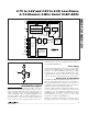

MAX1136–MAX1139
2.7V to 3.6V and 4.5V to 5.5V, Low-Power,
4-/12-Channel, 2-Wire Serial 10-Bit ADCs
2 _______________________________________________________________________________________
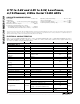
ABSOLUTE MAXIMUM RATINGS
ELECTRICAL CHARACTERISTICS
(V
DD
= 2.7V to 3.6V (MAX1137/MAX1139), V
DD
= 4.5V to 5.5V (MAX1136/MAX1138), V
REF
= 2.048V (MAX1137/MAX1139), V
REF
=
4.096V (MAX1136/MAX1138), C
REF
= 0.1µF, f
SCL
= 1.7MHz, T
A
= T
MIN
to T
MAX
, unless otherwise noted. Typical values are at
T
A
= +25°C. See Tables 1–5 for programming notation.)
Stresses beyond those listed under “Absolute Maximum Ratings” may cause permanent damage to the device. These are stress ratings only, and functional
operation of the device at these or any other conditions beyond those indicated in the operational sections of the specifications is not implied. Exposure to
absolute maximum rating conditions for extended periods may affect device reliability.
V
DD
to GND..............................................................-0.3V to +6V
AIN0–AIN11,
REF to GND............-0.3V to the lower of (V
DD
+ 0.3V) and 6V
SDA, SCL to GND.....................................................-0.3V to +6V
Maximum Current Into Any Pin .........................................±50mA
Continuous Power Dissipation (T
A
= +70°C)
8-Pin µMAX (derate 4.5mW/°C above +70°C) .............362mW
16-Pin QSOP (derate 8.3mW/°C above +70°C)........666.7mW
Operating Temperature Range ...........................-40°C to +85°C
Junction Temperature......................................................+150°C
Storage Temperature Range .............................-60°C to +150°C
Lead Temperature (soldering, 10s) .................................+300°C
PARAMETER
SYMBOL
CONDITIONS
MIN TYP MAX
UNITS
DC ACCURACY (Note 1)
Resolution 10 Bits
Relative Accuracy INL (Note 2) ±1 LSB
Differential Nonlinearity DNL No missing codes over temperature ±1 LSB
Offset Error ±1 LSB
Offset-Error Temperature
Coefficient
Relative to FSR 0.3
ppm/°C
Gain Error (Note 3) ±1 LSB
Gain-Temperature Coefficient Relative to FSR 0.3
ppm/°C
Channel-to-Channel Offset
Matching
±0.1
LSB
Channel-to-Channel Gain
Matching
±0.1
LSB
DYNAMIC PERFORMANCE (f
IN(SINE-WAVE)
= 10kHz, V
IN(P-P)
= V
REF
, f
SAMPLE
= 94.4ksps)
Signal-to-Noise Plus Distortion
SINAD
60 dB
Total Harmonic Distortion THD Up to the 5th harmonic -70 dB
Spurious Free Dynamic Range SFDR 70 dB
Full-Power Bandwidth SINAD > 57dB 3.0
MHz
Full-Linear Bandwidth -3dB point 5.0
MHz
CONVERSION RATE
Internal clock 6.8
Conversion Time (Note 4)
t
CONV
External clock
10.6
µs
Internal clock, SCAN[1:0] = 01 53
Internal clock, SCAN[1:0] = 00
CS[3:0] = 1011 (MAX1138/MAX1139)
53
Throughput Rate
f
SAMPLE
External clock
94.4
ksps
Track/Hold Acquisition Time
800
ns