
Owner manual

Note 1: For DC accuracy, the MAX1136/MAX1138 are tested at V
DD
= 5V and the MAX1137/MAX1139 are tested at V
DD
= 3V. All
devices are configured for unipolar, single-ended inputs.
Note 2: Relative accuracy is the deviation of the analog value at any code from its theoretical value after the full-scale range and
offsets have been calibrated.
Note 3: Offset nulled.
Note 4: Conversion time is defined as the number of clock cycles needed for conversion multiplied by the clock period. Conversion
time does not include acquisition time. SCL is the conversion clock in the external clock mode.
Note 5: A filter on the SDA and SCL inputs suppresses noise spikes and delays the sampling instant.
Note 6: The absolute input-voltage range for the analog inputs (AIN0–AIN11) is from GND to V
DD
.
Note 7: When the internal reference is configured to be available at AIN_/REF (SEL[2:1] = 11) decouple AIN_/REF to GND with a
0.01µF capacitor.
Note 8: ADC performance is limited by the converter’s noise floor, typically 300µV
P-P
.
Note 9: Measured as for the MAX1137/MAX1139
and for the MAX1136/MAX1138
Note 10: A master device must provide a data hold time for SDA (referred to V
IL
of SCL) in order to bridge the undefined region of
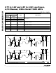
SCL’s falling edge (see Figure 1).
Note 11: C
B
= total capacitance of one bus line in pF.
Note 12: f
SCL
must meet the minimum clock low time plus the rise/fall times.
VVVV
V
VV
FS FS
REF
N
(. ) (. )
(. . )
55 45
21
55 45
−
−
−
[]
×
VVVV
V
VV
FS FS
REF
N
(. ) (. )
(. . )
36 27
21
36 27
−
−
−
[]
×
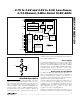
MAX1136–MAX1139
2.7V to 3.6V and 4.5V to 5.5V, Low-Power,
4-/12-Channel, 2-Wire Serial 10-Bit ADCs
_______________________________________________________________________________________ 5
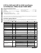
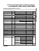
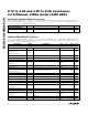
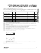
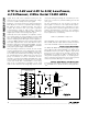
TIMING CHARACTERISTICS (Figure 1) (continued)
(V
DD
= 2.7V to 3.6V (MAX1137/MAX1139), V
DD
= 4.5V to 5.5V (MAX1136/MAX1138), V
REF
= 2.048V (MAX1137/MAX1139), V
REF
=
4.096V (MAX1136/MAX1138), C
REF
= 0.1µF, f
SCL
= 1.7MHz, T
A
= T
MIN
to T
MAX
, unless otherwise noted. Typical values are at
T
A
= +25°C. See Tables 1–5 for programming notation.)
PARAMETER
SYMBOL
CONDITIONS
MIN
TYP
MAX
UNITS
Rise Time of SCL Signal
(Current Source Enabled)
t
RCL
Measured from 0.3V
DD
to 0.7V
DD
20 80 ns
Rise Time of SCL Signal after
Acknowledge Bit
t
RCL1
Measured from 0.3V
DD
to 0.7V
DD
20 160 ns
Fall Time of SCL Signal t
FCL
Measured from 0.3V
DD
to 0.7V
DD
20 80 ns
Rise Time of SDA Signal t
RDA
Measured from 0.3V
DD
to 0.7V
DD
20 160 ns
Fall Time of SDA Signal t
FDA
Measured from 0.3V
DD
to 0.7V
DD
20 160 ns
Setup Time for STOP (P) Condition t
SU
,
STO
160
ns
Capacitive Load for Each Bus Line
C
B
400 pF
Pulse Width of Spike Suppressed
t
SP
(Notes 10 and 12) 0 10 ns