
User Manual

MAX1144/MAX1145
The user-programmable outputs are set to zero during
power-on reset or when RST goes low. During hardware
or software shutdown, P0, P1, and P2 are unchanged
and remain low-impedance.
Starting a Conversion
Start a conversion by clocking a control byte into the
device’s internal shift register. With CS low, each rising
edge on SCLK clocks a bit from DIN into the
MAX1144/MAX1145’s internal shift register. After CS
goes low or after a conversion or calibration completes,
the first arriving logic “1” is defined as the start bit of
the control byte. Until this first start bit arrives, any num-
ber of logic “0” bits can be clocked into DIN with no
effect. If at any time during acquisition or conversion
CS is brought high and then low again, the part is
placed into a state where it can recognize a new start
bit. If a new start bit occurs before the current conver-
sion is complete, the conversion is aborted and a new
acquisition is initiated.
Internal and External Clock Modes
The MAX1144/MAX1145 use either the external serial
clock or the internal clock to perform the successive-
approximation conversion. In both clock modes, the
external clock shifts data in and out of the
MAX1144/MAX1145. Bit 5 (INT/EXT) of the control byte
programs the clock mode.
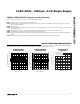
External Clock
In external clock mode, the external clock not only
shifts data in and out, but also drives the ADC conver-
sion steps.
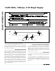
In short acquisition mode, SSTRB pulses high for one
clock period after the seventh falling edge of SCLK fol-
lowing the start bit. The MSB of the conversion is avail-
able at DOUT on the eighth falling edge of SCLK
(Figure 2).
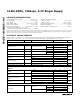
14-Bit ADCs, 150ksps, 3.3V Single Supply
10 ______________________________________________________________________________________
SCLK
DOUT
A/D
STATE
DIN
SSTRB
CS
418
START
M1 M0
P2
P1 P0
14
29 32
B2B12
B13
MSB
B11
B1
XX
B0
LSB
FILLED WITH
ZEROS
t
ACQ
ACQUISITION CONVERSIONIDLE IDLE
15
UNI/
BIP
INT/
EXT
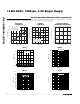
Figure 3. Long Acquisition Mode (32 Clock Cycles) External Clock
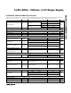
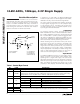
t
SDV
t
SSTRB
t
SSTRB
t
STR
P1 CLOCKED IN
SSTRB
SCLK
CS
Figure 4. External Clock Mode SSTRB Detailed Timing