
User Manual


MAX1144/MAX1145
14-Bit ADCs, 150ksps, 3.3V Single Supply
______________________________________________________________________________________ 11
SCLK
DOUT
DIN
SSTRB
CS
418
START
M1 M0
P2
P1 P0
9
21 24
B2B12
B13
MSB
B1
XX
B0
LSB
FILLED WITH
ZEROS
t
ACQ
t
CONV
UNI/
BIP
INT/
EXT
Figure 5. Internal Clock Mode Timing, Short Acquisition, Bipolar Mode
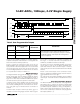
In long acquisition mode, SSTRB pulses high for one
clock period after the 15th falling edge of SCLK follow-
ing the start bit. The MSB of the conversion is available
at DOUT on the 16th falling edge of SCLK (Figure 3).
In external clock mode, SSTRB is high impedance
when CS is high (Figure 4). In external clock mode, CS
is normally held low during the entire conversion. If CS
goes high during the conversion SCLK is ignored until
CS goes low. This allows external clock mode to be
used with 8-bit bytes.
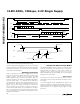
Internal Clock
In internal clock mode, the MAX1144/MAX1145 generate
their own conversion clock. This frees the microprocessor
from the burden of running the SAR conversion clock,
and allows the conversion results to be read back at the
processor’s convenience, at any clock rate up to 4MHz.
SSTRB goes low at the start of the conversion and goes
high when the conversion is complete. SSTRB will be
low for a maximum of 7µs, during which time SCLK
should remain low for best noise performance. An inter-
nal register stores data when the conversion is in
progress. SCLK clocks the data out of the internal stor-
age register at any time after the conversion is complete.
The MSB of the conversion is available at DOUT when
SSTRB goes high. The subsequent 13 falling edges on
SCLK shift the remaining bits out of the internal storage
register (Figure 5). CS does not need to be held low
once a conversion is started.
P0 CLOCKED IN
t
SSTRB
t
CONV
t
SCK
t
CSS
SSTRB
SCLK
NOTE: FOR BEST NOISE PERFORMANCE, KEEP SCLK LOW DURING CONVERSION.
t
CSH
CS
Figure 6. Internal Clock Mode SSTRB Detailed Timing