
User Manual

MAX1144/MAX1145
14-Bit ADCs, 150ksps, 3.3V Single Supply
_______________________________________________________________________________________ 7
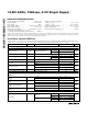
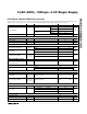
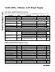
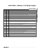
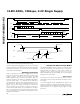
Pin Description
PIN NAME FUNCTION
1 REF ADC Reference Input. Connect a 2.048V voltage source to REF. Bypass REF to AGND with 4.7µF capacitor.
2AV
DD
Analog Supply. Connect to pin 4.
3 AGND Analog Ground. This is the primary analog ground (star ground).
4AV
DD
Analog Supply, 3.3V ±5%. Bypass AV
DD
to AGND (pin 3) with a 0.1µF capacitor.
5 DGND Digital Ground
6 SHDN Shutdown Control Input. Drive SHDN low to put the ADC in shutdown mode.
7 P2 User-Programmable Output 2
8 P1 User-Programmable Output 1
9 P0 User-Programmable Output 0
10 SSTRB
Serial Strobe Output. In internal clock mode, SSTRB goes low when the ADC begins a conversion and goes
high when the conversion is finished. In external clock mode, SSTRB pulses high for one clock period before
the MSB decision. It is high impedance when CS is high in external clock mode.
11 DOUT
Serial Data Output. MSB first, straight binary format for unipolar input, two’s complement for bipolar input.
Each bit is clocked out of DOUT at the falling edge of SCLK.
12 RST Reset Input. Drive RST low to put the device in the power-on default mode. See the Power-On Reset section.
13 SCLK
Serial Data Clock Input. Serial data on DIN is loaded on the rising edge of SCLK, and serial data is updated
on DOUT on the falling edge of SCLK. In external clock mode SCLK sets the conversion speed.
14 DGND Digital Ground. Connect to pin 5.
15 DV
DD
Digital Supply, 3.3V ±5%. Bypass DV
DD
to DGND (pin 14) with a 0.1µF capacitor.
16 DIN Serial Data Input. Serial data on DIN is latched on the rising edge of SCLK.
17 CS
Chip Select Input. Drive CS low to enable the serial interface. When CS is high DOUT is high impedance. In
external clock mode SSTRB is high impedance when CS is high.
18 CREF Reference Buffer Bypass. Bypass CREF to AGND (pin 3) with 1µF.
19 AGND Analog Ground. Connect to pin 3.
20 AIN Analog Input