
User Manual

MAX1144/MAX1145
Detailed Description
The MAX1144/MAX1145 ADCs use a successive-
approximation technique and input track/hold (T/H) cir-
cuitry to convert an analog signal to a 14-bit digital
output. The MAX1144/MAX1145 easily interface to
microprocessors (µPs). The data bits can be read
either during the conversion in external clock mode or
after the conversion in internal clock mode.
In addition to a 14-bit ADC, the MAX1144/MAX1145
include an input scaler, an internal digital microcontroller,
calibration circuitry, and an internal clock generator.
The input scaler for the MAX1144 enables conversion
of input signals ranging from 0 to +6V (unipolar input)
or ±6V (bipolar input). The MAX1145 accepts 0 to
+2.048V (unipolar input) or ±2.048V (bipolar input).
Input range is software selectable.
Calibration
To minimize linearity, offset, and gain errors, the
MAX1144/MAX1145 have on-demand software calibra-
tion. Initiate calibration by writing a control byte with bit
M1 = 0 and bit M0 = 1 (Table 1). Select internal or exter-
nal clock for calibration by setting the INT/EXT bit in the
control byte. Calibrate the MAX1144/MAX1145 with the
same clock mode used for performing conversions.
Offsets resulting from synchronous noise (such as the
conversion clock) are canceled by the MAX1144/
MAX1145’s calibration circuitry. However, because the
magnitude of the offset produced by a synchronous
signal depends on the signal’s shape, recalibration
may be appropriate if the shape or relative timing of the
clock, or other digital signals change, as may occur if
more than one clock signal or frequency is used.
Input Scaler
The MAX1144/MAX1145 have an input scaler, which
allows conversion of true bipolar input voltages while
operating from a single 3.3V supply. The input scaler
attenuates and shifts the input as necessary to map the
external input range to the input range of the internal
ADC. The MAX1144 analog input range is 0 to +6V
(unipolar) or ±6V (bipolar). The MAX1145 analog input
14-Bit ADCs, 150ksps, 3.3V Single Supply
8 _______________________________________________________________________________________
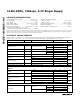
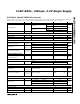
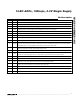
BIT NAME DESCRIPTION
7 (MSB) START The first logic “1” bit after CS goes low defines the beginning of the control byte.
6 UNI/BIP
1 = unipolar, 0 = bipolar. Selects unipolar or bipolar conversion mode. In unipolar mode, analog input
signals from 0 to +6V (MAX1144) or 0 to +VREF (MAX1145) can be converted. In bipolar mode, analog
input signals from –6V to +6V (MAX1144) or –VREF to +VREF (MAX1145) can be converted.
5 INT/EXT Selects the internal or external conversion clock. 1 = internal, 0 = external.
M1 M0 Mode
0 0 24 external clocks per conversion (short acquisition mode)4M1
0 1 Start calibration: starts internal calibration
1 0 Software power-down mode
3M0
1 1 32 external clocks per conversion (long acquisition mode)
2P2
1P1
0 (LSB) P0
These three bits are stored in a port register and output to pins P2, P1, P0 for use in addressing a mux
or PGA. These three bits are updated in the port register simultaneously when a new control byte is
written.
Table 1. Control Byte Format
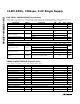
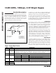
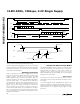
Figure 1. Equivalent Input Circuit
VOLTAGE
REFERENCE
BIPOLAR
UNIPOLAR
TRACK
S2
S3
S1 = BIPOLAR/UNIPOLAR
S2, S3 = T/H SWITCH
R2 = 7.6kΩ (MAX1144)
OR 2.5kΩ (MAX1145)
R3 = 3.9kΩ (MAX1144)
OR INFINITY (MAX1145)
HOLD
HOLD
T/H OUT
C
HOLD
32pF
R1
2.5kΩ
R2
R3
AIN
TRACK