
User Manual

range is 0 to +2.048V (unipolar) or ±2.048V (bipolar).
Unipolar and bipolar mode selection is configured with
bit 6 of the serial control byte (Table 1).
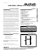
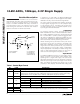
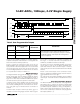
Figure 1 shows the equivalent input circuit of the
MAX1144/MAX1145. The resistor network on the analog
input provides ±16.5V fault protection. This circuit limits
the current going into or out of the pin to less than 2mA.
The overvoltage protection is active even if the device
is in a power-down mode, or if AV
DD
= 0.
Digital Interface
The digital interface pins consist of SHDN, RST, SSTRB,
DOUT, SCLK, DIN, and CS. Bringing SHDN low places
the MAX1144/MAX1145 in its 1.2µA shutdown mode. A
logic low on RST halts the MAX1144/MAX1145 opera-
tion and returns the part to its power-on-reset state.
In external clock mode, SSTRB is low and pulses high
for one clock cycle at the start of conversion. In internal
clock mode, SSTRB goes low at the start of the conver-
sion, and goes high to indicate that the conversion is
finished.
The DIN input accepts control byte data, which is
clocked in on each rising edge of SCLK. After CS goes
low or after a conversion or calibration completes, the
first logic “1” clocked into DIN is interpreted as the
START bit, the MSB of the 8-bit control byte.
The SCLK input is the serial-data-transfer clock which
clocks data in and out of the MAX1144/MAX1145.
SCLK also drives the ADC conversion steps in external
clock mode (see the Internal and External Clock Modes
section).
DOUT is the serial output of the conversion result.
DOUT is updated on the falling edge of SCLK. DOUT is
high impedance when CS is high.
CS must be low for the MAX1144/MAX1145 to accept a
control byte. The serial interface is disabled when CS is
high.
User-Programmable Outputs
The MAX1144/MAX1145 have three user-programma-
ble outputs: P0, P1, and P2. The power-on default state
for the programmable outputs is zero. These are push-
pull CMOS outputs suitable for driving a multiplexer, a
PGA or other signal preconditioning circuitry. Bits 0, 1,
and 2 of the control byte control the user-programma-
ble outputs (Tables 1, 2).
MAX1144/MAX1145
14-Bit ADCs, 150ksps, 3.3V Single Supply
_______________________________________________________________________________________ 9
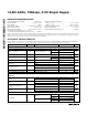
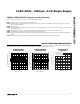
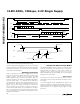
ACQUISITION CONVERSIONIDLE IDLE
SCLK
DOUT
A/D
STATE
DIN
SSTRB
CS
41812
START
M1 M0
P2
P1 P0
15
21 24
B10 B9B12 B11
B8
B7 B2
B13
MSB
B0
LSB
FILLED WITH
ZEROS
B1 X X
t
ACQ
UNI/
BIP
INT/
EXT
Figure 2. Short Acquisition Mode (24 Clock Cycles) External Clock
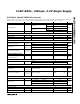
OUTPUT PIN
PROGRAMMED
THROUGH CONTROL
BYTE
POWER-ON OR
RST DEFAULT
DESCRIPTION
P2 Bit 2 0
P1 Bit 1 0
P0 Bit 0 0
User-programmable outputs follow the state of the control
byte’s three LSBs, and are updated simultaneously when a
new control byte is written. Outputs are push-pull. In hardware
and software shutdown, these outputs are unchanged and
remain low impedance.
Table 2. User-Programmable Outputs