
Instruction Manual

MAX11644/MAX11645
Low-Power, 1-/2-Channel, I
2
C, 12-Bit ADCs
in Ultra-Tiny 1.9mm x 2.2mm Package
_______________________________________________________________________________________ 3
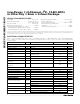
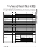
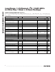
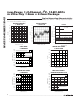
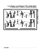
ELECTRICAL CHARACTERISTICS (continued)
(V
DD
= 2.7V to 3.6V (MAX11645), V
DD
= 4.5V to 5.5V (MAX11644), V
REF
= 2.048V (MAX11645), V
REF
= 4.096V (MAX11644),
f
SCL
= 1.7MHz, T
A
= T
MIN
to T
MAX
, unless otherwise noted. Typical values are at T
A
= +25°C, see Tables 1–5 for programming
notation.) (Note 1)
PARAMETER SYMBOL CONDITIONS MIN TYP MAX UNITS
ANALOG INPUT (AIN0/AIN1)
Unipolar 0 V
REFInput Voltage Range, Single-
Ended and Differential (Note 7)
Bipolar 0 ±V
REF
/2
V
Input Multiplexer Leakage
On/off leakage current, V
AIN
_ = 0 or V
DD
±0.01 ±1 μA
Input Capacitance C
IN
22 pF
INTERNAL REFERENCE (Note 8)
MAX11645 1.968 2.048 2.128
Reference Voltage V
REF
T
A
= +25°C
MAX11644 3.936 4.096 4.256
V
Reference-Voltage Temperature
Coefficient
TCV
REF
25 ppm/°C
REF Short-Circuit Current 2 mA
REF Source Impedance 1.5 k
EXTERNAL REFERENCE
REF Input Voltage Range V
REF
(Note 9) 1 V
DD
V
REF Input Current I
REF
f
SAMPLE
= 94.4ksps 40 μA
DIGITAL INPUTS/OUTPUTS (SCL, SDA)
Input-High Voltage V
IH
0.7 x V
DD
V
Input-Low Voltage V
IL
0.3 x V
DD
V
Input Hysteresis V
HYST
0.1 x V
DD
V
Input Current I
IN
V
IN
= 0 to V
DD
±10 μA
Input Capacitance C
IN
15 pF
Output Low Voltage V
OL
I
SINK
= 3mA 0.4 V
POWER REQUIREMENTS
MAX11645 2.7 3.6
Supply Voltage V
DD
MAX11644 4.5 5.5
V
Internal reference 900 1150
f
SAMPLE
= 94.4ksps
external clock
External reference 670 900
Internal reference 530
f
SAMPLE
= 40ksps
internal clock
External reference 230
Internal reference 380
f
SAMPLE
= 10ksps
internal clock
External reference 60
Internal reference 330
f
SAMPLE
=1ksps
internal clock
External reference 6
Supply Current I
DD
Shutdown (internal REF off) 0.5 10
μA
Power-Supply Rejection Ratio PSRR Full-scale input (Note 10) ±0.5 ±2.0 LSB/V