
Instruction Manual

General Description
The MAX1198 is a 3.3V, dual, 8-bit analog-to-digital con-
verter (ADC) featuring fully differential wideband track-
and-hold (T/H) inputs, driving two ADCs. The MAX1198
is optimized for low power, small size, and high-dynamic
performance for applications in imaging, instrumenta-
tion, and digital communications. This ADC operates
from a single 2.7V to 3.6V supply, consuming only
264mW, while delivering a typical signal-to-noise and
distortion (SINAD) of 48.1dB at an input frequency of
50MHz and a sampling rate of 100Msps. The T/H-driven
input stages incorporate 400MHz (-3dB) input ampli-
fiers. The converters may also be operated with single-
ended inputs. In addition to low operating power, the
MAX1198 features a 3.2mA sleep mode, as well as a
0.15µA power-down mode to conserve power during
idle periods.
An internal 2.048V precision bandgap reference sets
the full-scale range of the ADC. A flexible reference
structure allows the use of this internal or an externally
applied reference, if desired, for applications requiring
increased accuracy or a different input voltage range.
The MAX1198 features parallel, CMOS-compatible three-
state outputs. The digital output format can be set to two’s
complement or straight offset binary through a single con-
trol pin. The device provides for a separate output power
supply of 1.7V to 3.6V for flexible interfacing with various
logic families. The MAX1198 is available in a 7mm x 7mm,
48-pin TQFP package, and is specified for the extended
industrial (-40°C to +85°C) temperature range.
Pin-compatible lower speed versions of the MAX1198
are also available. Refer to the MAX1195 data sheet for
40Msps and the MAX1197 data sheet for 60Msps. In
addition to these speed grades, this family includes a
multiplexed output version (MAX1196, 40Msps), for
which digital data is presented time interleaved and on
a single, parallel 8-bit output port.
For a 10-bit, pin-compatible upgrade, refer to the
MAX1180 data sheet. With the N.C. pins of the
MAX1198 internally pulled down to ground, this ADC
becomes a drop-in replacement for the MAX1180.
Applications
Features
♦ Single 2.7V to 3.6V Operation
♦ Excellent Dynamic Performance
48.1dB/47.6dB SINAD at f
IN
= 50MHz/200MHz
66dBc/61.5dBc SFDR at f
IN
= 50MHz/200MHz
♦ -72dB Interchannel Crosstalk at f
IN
= 50MHz
♦ Low Power
264mW (Normal Operation)
10.6mW (Sleep Mode)
0.5µW (Shutdown Mode)
♦ 0.05dB Gain and ±0.1° Phase Matching
♦ Wide ±1V
P-P
Differential Analog Input Voltage
Range
♦ 400MHz -3dB Input Bandwidth
♦ On-Chip 2.048V Precision Bandgap Reference
♦ User-Selectable Output Format—Two’s
Complement or Offset Binary
♦ Pin-Compatible 8-Bit and 10-Bit Upgrades
Available
MAX1198
Dual, 8-Bit, 100Msps, 3.3V, Low-Power ADC
with Internal Reference and Parallel Outputs
________________________________________________________________ Maxim Integrated Products 1
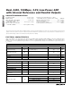
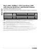
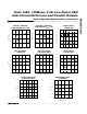
N.C.
N.C.
OGND
OV
DD
OV
DD
OGND
N.C.
N.C.
D0B
D1B
D2B
D3B
COM
V
DD
GND
INA+
INA-
V
DD
GND
INB-
INB+
GND
V
DD
CLK
1
2
3
4
5
6
7
8
9
10
11
12
36
35
34
33
32
31
30
29
28
27
26
25
TQFP-EP
GND
V
DD
GND
V
DD
T/B
SLEEP
PD
OE
D7B
D6B
D5B
D4B
13
14
15
16
17
18
19
20
21
22
23
24
48
47
46
45
44
43
42
41
40
39
38
37
REFN
REFP
REFIN
REFOUT
D7A
D6A
D5A
D4A
D3A
D2A
D1A
D0A
MAX1198
Pin Configuration
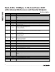
Ordering Information
19-2412; Rev 0; 4/02
For pricing, delivery, and ordering information, please contact Maxim/Dallas Direct! at
1-888-629-4642, or visit Maxim’s website at www.maxim-ic.com.
Functional Diagram and Pin Compatible Upgrades table
appear at end of data sheet.
*EP = Exposed paddle
Baseband I/Q Sampling
Multichannel IF Sampling
Ultrasound and Medical
Imaging
Battery-Powered
Instrumentation
WLAN, WWAN, WLL,
MMDS Modems
Set-Top Boxes
VSAT Terminals
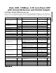
PART TEMP RANGE PIN-PACKAGE
MAX1198ECM -40°C to +85°C 48 TQFP-EP*