
Instruction Manual

MAX1198
Dual, 8-Bit, 100Msps, 3.3V, Low-Power ADC
with Internal Reference and Parallel Outputs
2 _______________________________________________________________________________________
ABSOLUTE MAXIMUM RATINGS
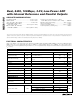
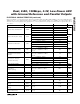
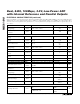
ELECTRICAL CHARACTERISTICS
(V
DD
= 3.3V, OV
DD
= 2.5V, 0.1µF and 2.2µF capacitors from REFP, REFN, and COM to GND; REFOUT connected to REFIN through a
10kΩ resistor, V
IN
= 2V
P-P
(differential with respect to COM), C
L
= 10pF at digital outputs, f
CLK
= 100MHz, T
A
= T
MIN
to T
MAX
, unless
otherwise noted. ≥+25°C guaranteed by production test, <+25°C guaranteed by design and characterization. Typical values are at
T
A
= +25°C.)
Stresses beyond those listed under “Absolute Maximum Ratings” may cause permanent damage to the device. These are stress ratings only, and functional
operation of the device at these or any other conditions beyond those indicated in the operational sections of the specifications is not implied. Exposure to
absolute maximum rating conditions for extended periods may affect device reliability.
V
DD
, OV
DD
to GND ...............................................-0.3V to +3.6V
OGND to GND.......................................................-0.3V to +0.3V
INA+, INA-, INB+, INB- to GND ...............................-0.3V to V
DD
REFIN, REFOUT, REFP, REFN,
COM, CLK to GND .................................-0.3V to (V
DD
+ 0.3V)
OE, PD, SLEEP, T/B, D7A–D0A,
D7B–D0B to OGND .............................-0.3V to (OV
DD
+ 0.3V)
Continuous Power Dissipation (T
A
= +70°C)
48-Pin TQFP (derate 12.5mW/°C above +70°C).........1000mW
Operating Temperature Range ...........................-40°C to +85°C
Junction Temperature......................................................+150°C
Storage Temperature Range .............................-60°C to +150°C
Lead Temperature (soldering, 10s) .................................+300°C
PARAMETER SYMBOL CONDITIONS MIN T YP MAX UNITS
DC ACCURACY
Resolution 8 Bits
Integral Nonlinearity INL f
IN
= 7.5MHz (Note 1) ±0.3 ±1 LSB
Differential Nonlinearity DNL
f
IN
= 7.5MHz, no missing codes guaranteed
(Note 1)
±0.2 ±1 LSB
Offset Error ±4%FS
Gain Error ±4%FS
Gain Temperature Coefficient ±100 ppm/°C
ANALOG INPUT
Differential Input Voltage Range V
DIFF
Differential or single-ended inputs ±1.0 V
Common-Mode Input Voltage
Range
V
CM
V
D D
/ 2
±0.2
V
Input Resistance R
IN
Switched capacitor load 57 kΩ
Input Capacitance C
IN
5pF
CONVERSION RATE
Maximum Clock Frequency f
CLK
100 MHz
Data Latency 5
Clock
Cycles
DYNAMIC CHARACTERISTICS (f
CLK
= 100MHz, 4096-point FFT)
f
INA or B
= 7.5MHz at -1dB FS 48.5
f
INA or B
= 20MHz at -1dB FS 47.0 48.3
f
INA or B
= 50MHz at -1dB FS 48.3
Signal-to-Noise Ratio SNR
f
INA or B
= 115.1MHz at -1dB FS 48.1
dB