
Instruction Manual

MAX1198
Dual, 8-Bit, 100Msps, 3.3V, Low-Power ADC
with Internal Reference and Parallel Outputs
_______________________________________________________________________________________ 3
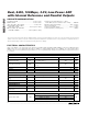
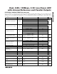
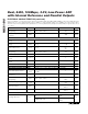
ELECTRICAL CHARACTERISTICS (continued)
(V
DD
= 3.3V, OV
DD
= 2.5V, 0.1µF and 2.2µF capacitors from REFP, REFN, and COM to GND; REFOUT connected to REFIN through a
10kΩ resistor, V
IN
= 2V
P-P
(differential with respect to COM), C
L
= 10pF at digital outputs, f
CLK
= 100MHz, T
A
= T
MIN
to T
MAX
, unless
otherwise noted. ≥+25°C guaranteed by production test, <+25°C guaranteed by design and characterization. Typical values are at
T
A
= +25°C.)
PARAMETER SYMBOL CONDITIONS MIN T YP MAX UNITS
f
INA or B
= 7.5MHz at -1dB FS 48.3
f
INA or B
= 20MHz at -1dB FS 46.5 48.2
f
INA or B
= 50MHz at -1dB FS 48.1
Signal-to-Noise and Distortion SINAD
f
INA or B
= 115.1MHz at -1dB FS 48
dB
f
INA or B
= 7.5MHz at -1dB FS 67
f
INA or B
= 20MHz at -1dB FS 60 67
f
INA or B
= 50MHz at -1dB FS 66
Spurious-Free Dynamic Range SFDR
f
INA or B
= 115.1MHz at -1dB FS 65
dBc
f
INA or B
= 7.5MHz at -1dB FS - 67
f
INA or B
= 20MHz at -1dB FS - 67
f
INA or B
= 50MHz at -1dB FS - 67
Third-Harmonic Distortion HD3
f
INA or B
= 115.1MHz at -1dB FS - 66
dBc
Intermodulation Distortion
(First Five Odd-Order IMDs)
IMD
f
IN1(A or B)
= 1.989MHz at -7dB FS
f
IN2(A or B)
= 2.038MHz at -7dB FS
(Note 2)
- 69.5 dBc
Third-Order Intermodulation
Distortion
IM3
f
IN1(A or B)
= 1.989MHz at -7dB FS
f
IN2(A or B)
= 2.038MHz at -7dB FS
(Note 2)
- 80 dBc
f
INA or B
= 7.5MHz at -1dB FS - 66
f
INA or B
= 20MHz at -1dB FS - 67 - 57
f
INA or B
= 50MHz at -1dB FS - 64
Total Harmonic Distortion
(First Four Harmonics)
THD
f
INA or B
= 115.1MHz at -1dB FS - 58
dBc
Small-Signal Bandwidth Input at -20dB FS, differential inputs 500 MHz
Full-Power Bandwidth FPBW Input at -1dB FS, differential inputs 400 MHz
Gain Flatness
(12MHz Spacing)
f
IN1(A or B)
= 106MHz at -1dB FS
f
IN2(A or B)
= 118MHz at -1dB FS
(Note 3)
0.05 dB
Aperture Delay t
AD
1ns
Aperture Jitter t
AJ
1dB SNR degradation at Nyquist 2 ps
RMS
Overdrive Recovery Time For 1.5 × full-scale input 2 ns
IN T ER N A L REF ER EN C E ( RE FIN = RE FOU T thr oug h 10kΩ r esi stor ; RE FP , RE FN , and C OM l evel s ar e g ener ated i nter nal l y.)
Reference Output Voltage V
REFOUT
(Note 4)
2.048
± 3%
V
Positive Reference Output
Voltage
V
REFP
(Note 5) 2.162 V
Negative Reference Output
Voltage
V
REFN
(Note 5) 1.138 V
Common-Mode Level V
COM
(Note 5)
V
D D
/ 2
±0.1
V